OFC50: The Era of High-Speed Silicon Photonics Has Arrived! TSMC’s SiN Waveguide Powers NVIDIA’s Photonic Ambitions
Original Articles by SemiVision Research (OFC50)


SemiVision Research believes that the next phase of collaboration between NVIDIA and TSMC in silicon photonics technology will focus on optimizing edge couplers to achieve higher bandwidth optical engines. Specifically, improvements will be made in the coupling design between waveguides and optical fibers, involving precise adjustments to reverse taper structures, careful selection of dielectric layer materials, and substrate undercut techniques. These efforts will significantly reduce coupling losses and enhance optical signal stability. As single-channel bandwidth scales up from 200G to 400G and beyond, reducing insertion losses and polarization-dependent losses (PDL) at the edge coupler becomes crucial. This progress will enable integration of more wavelengths and higher-density optical channels within the same optical engine, thereby expanding the overall performance and competitiveness of optoelectronic integration modules for data centers, AI computing, and HPC applications.
In recent years, TSMC has published numerous research papers and patents aimed at strengthening silicon photonics integration. According to TSMC’s technology forums, the ultimate goal of silicon photonics is to achieve chip-to-chip (C2C) interconnections. However, this represents a significant challenge, demanding substantial investment in time, space, and highly integrated packaging solutions. TSMC’s frequent publications on advanced silicon photonics techniques demonstrate its proactive strategy for future development. Silicon photonics must leverage the advantages of optical signals but also rely on efficient electrical signal transmission, highlighting the importance of serializer-deserializer (SerDes) technology. Additionally, for high-frequency transmission, signal amplification is essential, thus necessitating close attention to transimpedance amplifiers (TIA), such as those utilizing SiGe BiCMOS processes.

Research Background and Motivation
Silicon photonics (SiPh), characterized by its high bandwidth, energy efficiency, and scalability, has increasingly attracted interest from data centers, high-performance computing (HPC), artificial intelligence (AI), and 5G/6G communication sectors. Leveraging mature CMOS fabrication processes, SiPh platforms exhibit not only superior performance but also cost advantages associated with large-scale production.
Currently, TSMC primarily utilizes a 65nm CMOS process for SiPh device fabrication. However, modulators predominantly based on microring structures present significant lithography challenges for foundries, due to strict requirements on lithography windows, process tolerance, critical dimension (CD) control, and etch control.
To fulfill future bandwidth demands of data centers, photonic integrated circuits (PICs) must incorporate:
Capability for multiple wavelength channel transmission • High optical power handling (~21 dBm), to support an increased number of waveguide splits, evolving from the current mainstream 1:4 split to 1:8 or even higher (such as 1:16), imposing greater challenges on fabrication technology. • Advancement from current 200G/lane to 400G/lane transmission rates, accompanied by necessary upgrades in SerDes technology from existing 224G to 448G. Presently, only Broadcom demonstrates capability in 448G SerDes technology, while Marvell and MediaTek (MTK) remain primarily at 224G, necessitating continued monitoring of Broadcom's developments to achieve 400G/lane implementation.

Moreover, future PIC platforms must effectively support advanced technologies like wavelength division multiplexing (WDM) and pulse amplitude modulation (PAM4), crucial for overcoming traditional optical communication challenges such as bandwidth bottlenecks, signal density limitations, and excessive power consumption. In a previous article, SemiVision Research discussed why Nvidia and Broadcom chose different design approaches for CPO switches. For more details, please refer to the link below.
Conventional pure silicon (Si) devices suffer significant optical losses at high power due to two-photon absorption (TPA) and free-carrier absorption (FCA), alongside high thermal sensitivity attributed to their elevated thermo-optic coefficient (~1.8×10⁻⁴ /K).
In contrast, silicon nitride (SiN) demonstrates a lower thermo-optic coefficient (~2.5×10⁻⁵ /K) and reduced nonlinear losses, effectively handling high optical power, thus positioning SiN as an ideal complementary material for SiPh platforms. Nonetheless, achieving high-performance, uniform SiN devices on a 300mm wafer manufacturing platform remains technically challenging.
Therefore, this research aims to integrate high-quality SiN thin films, produced through advanced plasma-enhanced chemical vapor deposition (PECVD), into existing silicon photonic platforms, systematically validating photonic component performance, process uniformity, and reliability.


For Paid Members , SemiVision Research will discuss following topics:
The Rise of Photonic AI: TSMC’s SiN Technology Empowers NVIDIA’s Optical Ambitions
Improvement of SiN Photonic Component Performance
SiN Waveguide Bend Design
Improvement of SiN-to-Si Waveguide Transition Components
Optimization of SiN Edge Coupler (EC)
Research Conclusion
TSMC SoIC-X COUPE Roadmap and plaining to Optical I/O for Feynman
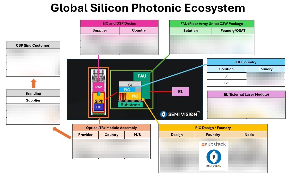
Global Silicon Photonic Ecosystem


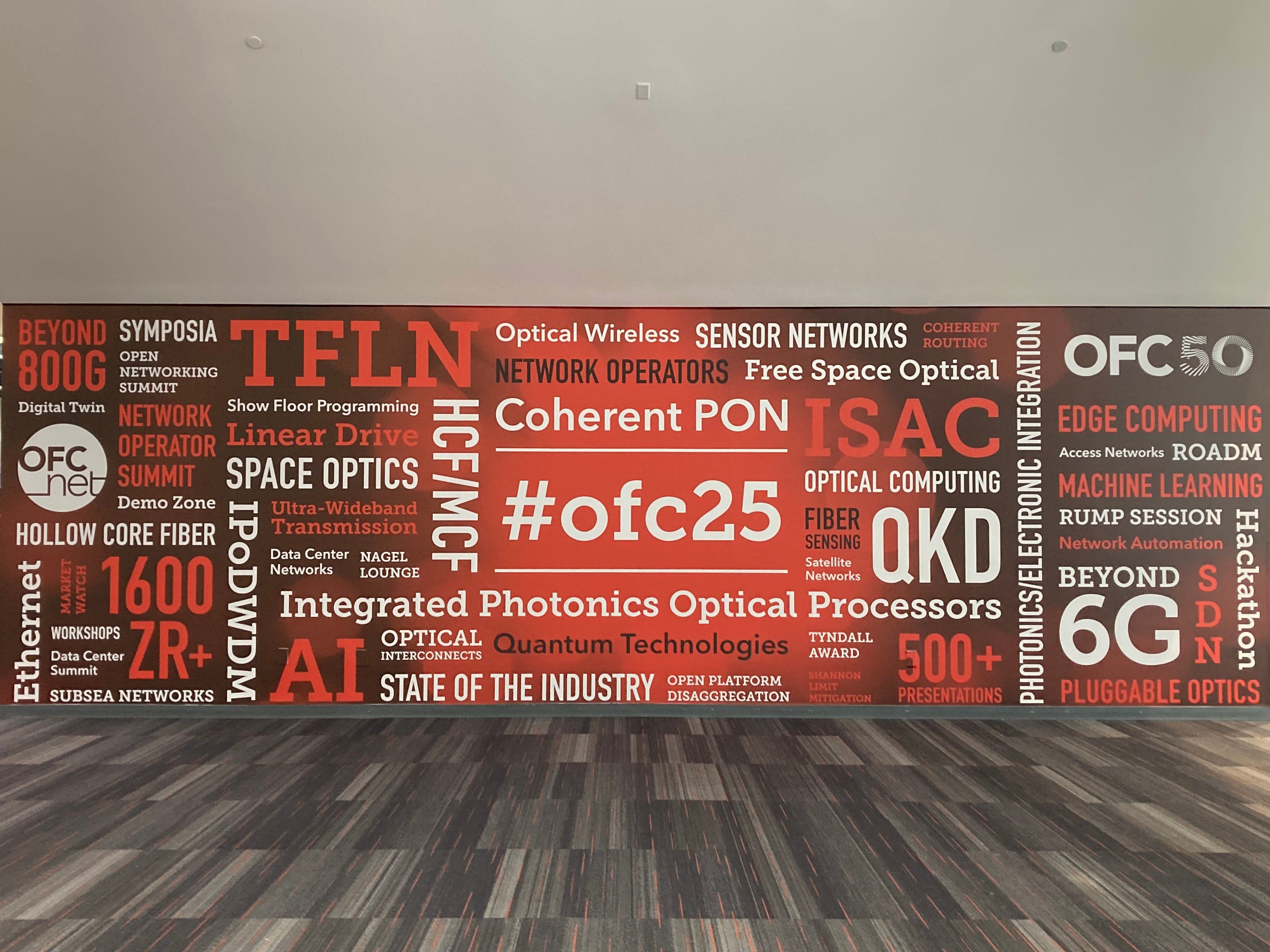
For OFC 50 , the hot topics can be discussed.
NVIDIA
• M4H.1:Large Scale AI Systems with Photonic Connectivity
• Tu2C.3:Translating AI/ML System Architecture Into Optical Requirements
• W3A.1:The Copper Behind Blackwell: Understanding Today’s Copper Scale-up Networks


Meta

• W1A.1:Embracing the AI Era: Optical Network Evolution to Scale the Backbone

• W1C.1:Technologies and Challenges for Pb/s Submarine Cable Deployment
• M4H.6:Impact of Optical Circuit Switching on AI Clusters
• Th3A.2:Scaling ML Workloads with Google’s Evolving Datacenter Network Architecture

• M3A.3:AIOps: The Autonomous Network Journey
• Tu2G.1:Manufacturable Inverse Designed Si Photonic Devices
Amazon
• M2H.6:Next-Generation Data Center Interconnects in the Age of AI
Microsoft


• M4C.4:From 400G to 1600G - Cloud Scale Deployment and Intelligent Operation of Inter-Datacenter Coherent Links
• Tu1A:Scaling Data Centers Is in Conflict with Increasing Interface Speeds
• Tu3I.1:Reliable Deployment and Operation of 400ZR Pluggable Optics for DCI at Hyperscale
• W4D.1:Analog Optical Computing for Sustainable AI and Beyond
Huawei

• M3A.6:Operations Science and Automation in Optical Networks: From Machine Learning to Generative AI
• Th3A.1:Evolution of Optical Network for Ubiquitous AI
Cisco
• Tu2C.2:LPO Technology: System Integration Insights, Progress, and Challenges
TSMC
• Tu3G.1:TSMC in the Silicon Photonics Era - an Electrical Perspective
Intel

• Tu3G.2:Intel 300mm Heterogeneously Integrated Silicon Photonics Technology: a Review of Recent Progress
IMEC

• Tu2C.4:Silicon Photonics and Advanced 3-D Assembly for Short-Reach Optical Interconnects
Hewlett Packard Labs
• W3D.6:In-Memory Optical Computing with Non-Volatile Silicon Photonic Memory
SPIL
• W4A.4:Advanced Packaging Solution for Co-Packaged Optics
ASE
• Th3H.5:Latest Advanced Packaging Solutions for AI
IBM
• Th3H.4:Photonic Modules with High Density Polymer Waveguide Interface
Corning
• M4F.5:Wavefront Control with Metasurfaces for Optical Fiber Connectivity
• Th3H.1:High-Density Evanescent Chip Coupling with Detachable Fiber Connector for Co-Packaged Optics
Furukawa Electric
• Tu3G.3:High Speed Optical Interconnect Technologies for AI/ML Applications
Ayar Labs

• Th3H.2:Connectorized Optical I/O Chiplet with v-Groove for AI and High Performance Computing
Lightmatter
• Tu3J.6:Monolithically Integrated Microring Transmitter and Receiver for High-Density 3D CoPackaged Optics
• Th1F.2:Chip-to-Chip Photonic Connectivity in Multi-Accelerator Servers for ML
Celestial AI
• W3D.1:Photonic Fabric for Memory and Compute Disaggregation
• Th1F.3:A 50 Gb/s WDM Silicon Photonic Ternary Content Addressable Memory Cell
Xscape
• W1E.1:Order-Preserving Channel Calibration of Kerr Comb–Driven Microresonator-Based DWDM Link
• W2A.21:Tapered-Hybrid Bend, Interior-Ridge Modulator and Filter Supporting Tbps-Scale Links
Nubis
• W1C.5:Real-Time 1.6-Tbps Transmission Over 10 km for 6G Fronthaul in Co-Packaged Optics Radio Access Networks Using Eye-Safe Standard-Single-Mode-Fiber-Fed Remote Laser Sources
SCINTIL Photonics
• W3A.4:Integrated Versus External Laser Sources in Pluggable and Co-Packaged Optics Applications
OpenLight
• M3K.3:Silicon Photonics Platform with Heterogeneously Integrated Lasers and EAMs for 1.6/3.2T
Quintessent
• W1G.3:Multi-Wavelength Quantum Dot Comb Lasers
Lucidean
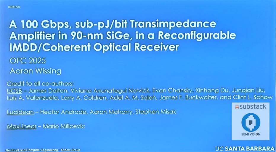
• M2H.3:A 100 Gbps, sub-pJ/bit Transimpedance Amplifier in 90-nm SiGe in a Reconfigurable IMDD/Coherent Optical Receiver
Singularity Photonics
• Tu3G.5:Optical Interconnects for AI Computing Applications
Teramount
• W4A.3:Scalable Detachable Fiber Connectivity for Seamless Integration with Advanced Semiconductor Packaging
Other key informations , you have to know from OFC50