

2025 CPO Heterogeneous Integration Technology Forum
Original Articles by SemiVision Research (Taiwan Technology Forum)

The 2025 CPO Heterogeneous Integration Technology Forum covered a wide range of diverse topics, with a primary focus on the challenges of testing and packaging for Co-Packaged Optics (CPO).
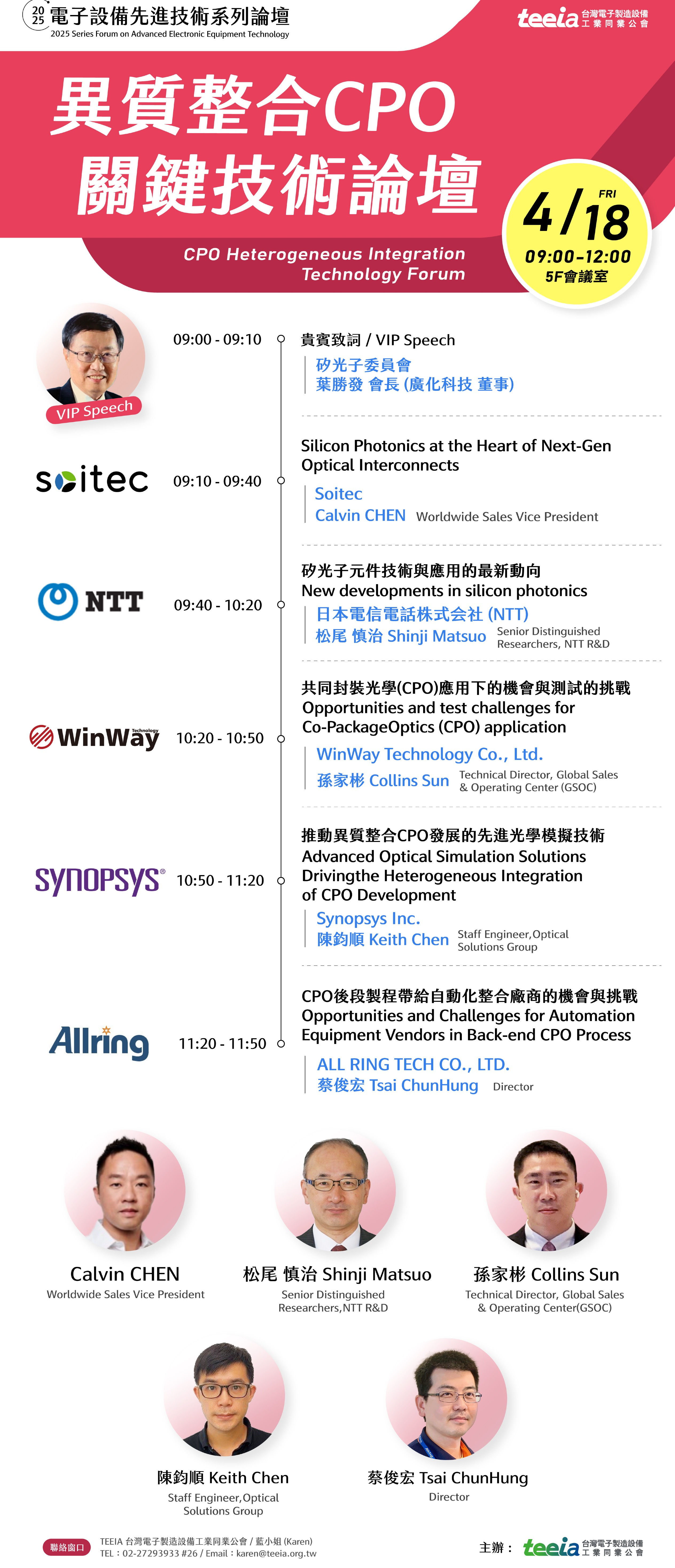
The organizer, TEEIA, invited several influential companies to explain the concept of Heterogeneous Integration and how it can be applied to Co-Packaged Optics (CPO). Featured keynote speakers included SOITEC, NTT, WinWay, Synopsys, and Allring.
SOITEC: The Foundational Technology Hub of the Silicon-Based World and the Silent Enabler of the Silicon Photonics Era
SOITEC, a France-based advanced materials engineering company founded in 1992, has positioned itself as the global leader in the development and manufacturing of Silicon-On-Insulator (SOI) wafers. Headquartered in Grenoble, with multiple production sites worldwide, the company is best known for its proprietary Smart Cut™ wafer bonding and layer transfer technology. This enables the high-precision transfer of ultra-thin layers of silicon or other materials onto insulator substrates, forming robust, highly uniform wafer platforms ideally suited for advanced semiconductor processing.
SOITEC’s engineered substrates are critical foundation materials adopted by leading foundries and system providers, including GlobalFoundries, Samsung, Tower Semiconductor, and Intel. Its materials support diverse application domains such as RF, low-power logic, image sensing, MEMS, automotive electronics, and increasingly, silicon photonics—where its impact is especially profound.
Through differentiated product lines such as RF-SOI, FD-SOI, POI (Piezoelectric-on-Insulator), and Photonic SOI, SOITEC strategically addresses the wide-ranging semiconductor demands of mobile communication, IoT, AI, automotive, and data centers.
In silicon photonics (SiPh), SOITEC plays a pivotal enabling role. Its Photonic SOI wafers, with ultra-thin top silicon layers (typically <220nm) and ultra-uniform low-defect BOX (Buried Oxide) structures, are ideal for single-mode waveguides with low insertion loss. These wafers substantially reduce coupling loss and manufacturing variability, making them the industry’s preferred platform for 300mm SiPh mass production.
From Intel’s SiPh TX/RX, Tower’s PH18 platform, to GlobalFoundries’ Fotonix™ process, SOITEC’s photonic-grade SOI wafers serve as the essential foundation. These platforms, in turn, power key applications such as LPO modules, CPO switches, high-speed AOCs, 800G/1.6T connectivity, and photonic packaging systems, all of which are integral to upgrading the AI data center and HPC infrastructure.
Beyond standard SOI wafers, SOITEC is actively developing next-generation material platforms, including:
Thick BOX wafers for enhanced optical-electrical coupling and reduced loss;
Custom top silicon thickness options for multi-wavelength/multi-mode systems;
InP-on-Si and III-V hetero-integration substrates for integrated light sources;
New optical-thermal coupling substrates to support SiPh SoCs, multi-layer interposers, and photonic-electronic heterogeneous integration.
SOITEC also collaborates with major research institutes and ecosystem players such as CEA-Leti, imec, imep, STMicroelectronics, and GlobalFoundries, co-developing material stacks targeting cross-domain applications in AI, telecommunications, automotive, and sensing.
The company’s 300mm SOI fabs in Singapore and Bernin (France) support tens of thousands of wafers per month and are undergoing further expansion to meet explosive growth in SiPh and RF demand. With its innovation-driven strategy, SOITEC is not just a material provider but a strategic pillar of the semiconductor ecosystem, playing a vital role in enabling optical interconnects, photonic packaging, CPO switches, and even photonic computing architectures.
As the industry enters the post-Moore era, SOITEC is poised to become a core enabler of heterogeneous integration and optoelectronic convergence, accelerating the commercialization of next-generation technologies.

For Paid Members, SemiVision will provide a curated summary of key takeaways from this talk. We will also conduct follow-up in-depth analysis on the topics presented by the speakers at this forum.
This article focuses on SOITEC, highlighting their presentation at the event. Exclusive photos and selected slides from the talk will be shared with our paid members.
SOITEC: The Core Materials Partner Powering Silicon Photonics at Scale
Key Material Characteristics and Technical Advantages
Value Extension into CPO and Advanced Packaging
The Invisible Backbone of the Global Silicon Photonics Ecosystem
GlobalFoundries Fotonix™: Deep Integration with Soitec
Tower Semiconductor PH18: A Backbone for Mid-Range Optical Communication
CEA-Leti & imec: Core Material Providers for Europe’s Photonics R&D Chain
Intel: Early-Stage SiPh Prototyping and Integration with Soitec
Enabling CPO, LPO, and AI Photonic Systems: The Critical Materials Platform
Key Material Innovations and Advantages in Photonic wafer
Strategic Implications in Soitec
Future Outlook: Advancing Toward Heterogeneous Integration and 3D Photonic Packaging
Strategic Outlook: From Material Supplier to Integration Enabler
Closing Thought: It All Starts with Silicon