


2025 Touch Taiwan Forum : CoPoS Opportunities and challenges
Original Article by SemiVision Research

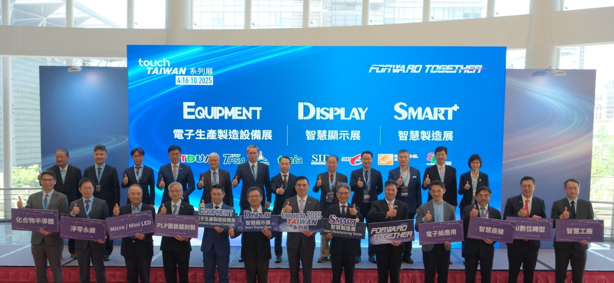
The 2025 Touch Taiwan series exhibition officially opened today (April 16) at the Taipei Nangang Exhibition Center and will run through April 18. Centered around the theme “Forward Together,” the event highlights the integration of the panel industry’s transformation with advanced packaging technologies, with a particular emphasis on the development and applications of FOPLP (Fan-Out Panel Level Packaging).
Exhibition Highlights
-FOPLP Technology Zone and Forum
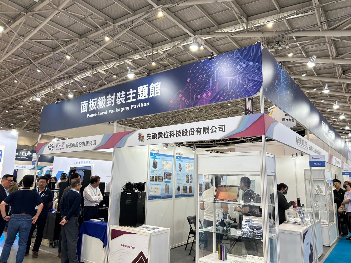
For the first time, a dedicated "Panel Level Packaging (PLP) Zone" has been established, showcasing advanced process technologies such as Redistribution Layer (RDL), etching, laser processing, and Through-Glass Via (TGV).
A “FOPLP Advanced Packaging Technology Trend Seminar” is also being held, featuring industry leaders such as ASE Group, Unimicron, and Innolux to share insights on real-world applications and technical challenges.
-Industry Transformation and Cross-Sector Collaboration
Innolux presents its latest advancements in FOPLP technology, highlighting applications in automotive and smartphone markets.
Unimicron explores the ongoing technical transformation of FOPLP in semiconductor packaging and its future outlook.
-International Participation and Technical Exchange
This year’s exhibition welcomes 328 leading companies from 10 countries, with a total of 920 booths, marking a 10% growth compared to last year.
Nearly 30 international forums are being held, covering topics such as e-paper, Micro LED, AI, PLP, and silicon photonics, promoting global technology exchange and collaboration.
The 2025 Touch Taiwan exhibition officially kicked off today, with this year’s theme centered on how the display industry can transition into the advanced packaging era through technological transformation. One of the most anticipated highlights is the dedicated zone and industry forum for FOPLP (Fan-Out Panel Level Packaging). The event clearly showcases the active participation of leading display and packaging companies such as Innolux and Unimicron, signaling a growing trend of cross-sector integration between display and semiconductor packaging technologies.
SemiVision Research is participating in the event to closely track the potential industrial pathway from display technology transformation to semiconductor packaging.
It’s important to note that advanced packaging is not simply an upgrade from traditional IC packaging—it has become an essential component in modern AI chip architectures. As demands for high bandwidth, low power consumption, and efficient thermal dissipation continue to rise, advanced packaging has become a foundational element in mainstream GPU and ASIC design.

One of the most prominent examples is TSMC’s CoWoS (Chip on Wafer on Substrate) technology, which has successfully integrated HBM (High Bandwidth Memory) with large-scale AI accelerator chips. This innovation has reshaped the mainstream paradigm of chip design and packaging in the AI era.

Nvidia’s Update on TSMC’s Advanced Packaging - CoWoS and SoIC
To gain a deeper understanding of this architecture, it is essential to emphasize the critical role played by the interposer. The interposer serves as a high-speed communication bridge between the GPU and HBM, and it is also one of the most expensive and complex components in the entire module design. It demands extremely high standards in signal integrity, thermal diffusion, and micro-bump pitch accuracy. This is precisely one of the reasons why TSMC’s CoWoS technology stands out—it not only enables production-grade interposer processes but also supports a complete manufacturing and testing supply chain.

According to research by SemiVision, TSMC is currently launching a Mini Line (pilot production line) for CoPoS (Chip on Panel on Substrate) at its advanced packaging (AP) site in Zhunan.

For Paid Members ,SemiVision will discuss topics on
TSMC CoPoS Status Updated
Key Material and Design Challenges of CoWoS-R
CoWoS-L: TSMC’s Current Flagship Advanced Packaging Node
CoPoS: TSMC’s Officially Defined Panel-Level Packaging Architecture
TSV vs. TGV Process Comparison and Physical Challenge Analysis
New Challenges in SI/PI and Build-Up Film

SemiVision will provide deeper analysis of the topics discussed at this year's Touch Taiwan forum. Stay tuned and subscribe to follow our updates!
