

2026 NVIDIA Silicon Photonics 3D Stacking and DWDM Half-Rate Optical Link Technology
Original Article By SemiVision Reserach [Reading time: 30mins]


NVIDIA Unveils a Breakthrough Silicon Photonics Paper at ISSCC 2026
SemiVision Provides an In-Depth Analysis of the Core Architecture
At ISSCC 2026 (International Solid-State Circuits Conference), NVIDIA presented a landmark paper titled:
“A 32Gb/s/λ 256Gb/s/Fiber Half-Rate Bandpass-Filtered Clock-Forwarding DWDM Optical Link in a 3D-Stacked 7nm EIC/65nm PIC Technology.”
This publication formally reveals the technological blueprint behind NVIDIA’s next-generation AI infrastructure interconnect strategy.
Following an in-depth technical review, SemiVision concludes that this work is far more than a high-speed optical link design. Rather, it represents a strategic declaration of NVIDIA’s architectural direction for scalable AI interconnect systems.
Introduction: Data Interconnect Challenges in the AI Era
As the scale of artificial intelligence models grows exponentially, the rate of data exchange between computing resources increasingly becomes a bottleneck for overall system performance. Deep learning training requires hundreds—or even thousands—of GPUs or accelerators to work collaboratively, and these computing units must transfer massive volumes of weights, gradients, and activation data at very high speed.
Traditional electrical interconnects (such as PCIe or high-speed chip-to-chip links) encounter fundamental challenges when pushing beyond 100 Gb/s, including impedance mismatch, signal-integrity degradation, and sharply rising power consumption. To overcome these limitations, the industry has begun exploring optical interconnects based on silicon photonics, along with Dense Wavelength Division Multiplexing (DWDM) technologies.
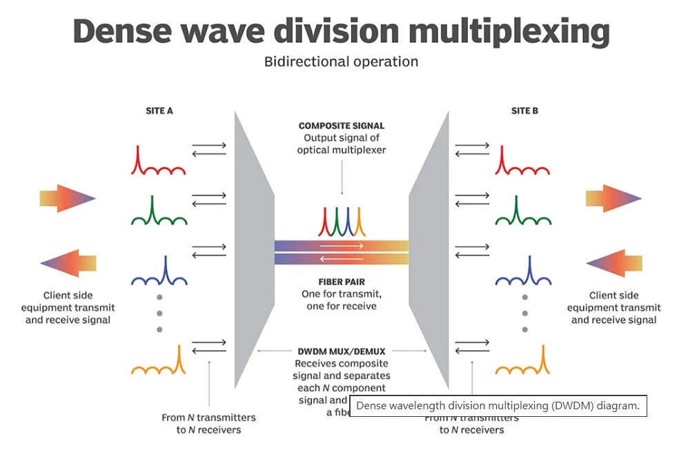
By leveraging the ability of optical fibers to carry multiple wavelengths simultaneously, these approaches distribute data across multiple lower-speed wavelength channels rather than relying on a single ultra-high-speed lane. This strategy avoids the extremes of single-channel transmission while achieving a better balance among energy efficiency, scalability, and latency.
Challenges of Traditional High-Speed Electrical I/O
As 56 Gb/s, 112 Gb/s, and even 224 Gb/s channels emerge, the industry has broadly adopted higher-order Pulse Amplitude Modulation (PAM4, 4-level PAM) to increase bit rates. However, the increased number of symbol levels in PAM4 significantly raises signal-to-noise ratio (SNR) requirements, leading to reduced receiver sensitivity.
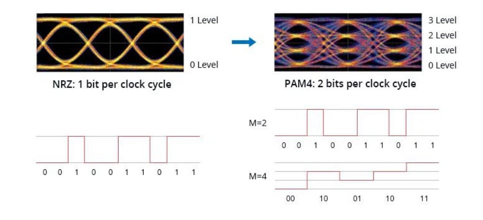
For example, achieving a 224 Gb/s channel requires a symbol rate of 112 Gbaud—effectively doubling the bandwidth. This places extremely stringent demands on a channel’s high-frequency response, crosstalk suppression, and equalization algorithms. In addition, even under optimal conditions, PAM4 exhibits a native bit error rate (BER) on the order of 1E-4 to 1E-6, making forward error correction (FEC) mandatory to reach the system-level requirement of 1E-12 or lower. FEC itself typically introduces more than 10 ns of additional latency.
These combined factors make ultra-high-speed electrical I/O increasingly difficult to scale in large-scale AI systems while simultaneously meeting the requirements for low latency and high energy efficiency.


For further reading on Co-Packaged Optics (CPO), please refer to the following articles.
In today’s era of explosive growth in AI training and inference workloads, data-center interconnects are under unprecedented pressure. As model parameter counts continue to scale and GPU clusters routinely expand to thousands of devices operating in parallel, interconnect bandwidth, density, and energy efficiency have become decisive bottlenecks for overall system performance.
