Behind the Yield: Exploring D₀ Challenges in TSMC × NVIDIA AI Chip Production
Original Article by SemiVision Research (TSMC / Nvidia)

In the age of AI supercomputing, die size is no longer limited by design ambition, but by manufacturability. Nowhere is this more evident than in NVIDIA’s massive AI accelerators—such as the H100, GB200, and future Blackwell-class architectures—which push the limits of logic density, power, and area. These cutting-edge chips rely heavily on TSMC’s ability to control defect density (D₀) during both early development and mass production.
While the industry often focuses on transistor counts and compute throughput, the less visible battle is fought in yield engineering—where every marginal improvement in D₀ translates into billions of dollars saved or lost in wafer costs. This article explores the intricate relationship between defect density, die area, process maturity, and yield trajectory, shedding light on how TSMC enables NVIDIA’s AI chip roadmap by mastering the art and science of D₀ suppression.
In a previous article, SemiVision introduced the concept of defect density, commonly referred to as D₀, which generated significant interest and questions from our readers. In response, this article aims to provide a more detailed explanation of the physical meaning and mathematical foundations of D₀, and its pivotal role in chip design and yield modeling.
D₀ is not just a statistical metric—it is a critical indicator that links process quality with economic viability. Here, we will explore its unit definition, its role in yield prediction models (such as the Poisson yield model), and how it is practically derived in real-world manufacturing scenarios. Our goal is to help readers gain a comprehensive understanding of this fundamental parameter in advanced semiconductor fabrication.

For Paid Members, SemiVision will discuss topics on
Understanding Defect Density
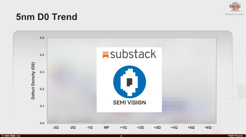
The Critical Link Between Defect Density (D₀) and Process Maturity — A Case Study on TSMC’s 5nm Node
Extended Insight: D₀ × Die Size Determines the Commercial Feasibility of Chips
D₀ as the Bridge Between Advanced Process Technology and Commercial Silicon
A Deep Dive into AI Chip Manufacturability: The Interplay of Defect Density and Die Area ( Nvidia ,AMD, Intel , Apple )
Why TSMC’s N5 Node Achieved Stable Low Defect Density Faster Than N7 and N10