

Breaking the AI Cooling Barrier: How TSMC and NVIDIA Tackle Next-Gen Chip Thermal Challenges
Original Article by SemiVision Research (TSMC, Nvidia, Henkel , Indium Corp.)

As artificial intelligence (AI) accelerators continue to grow in complexity and power density, thermal management has become one of the most critical bottlenecks in semiconductor design. According to industry data, heat accounts for over 55% of all electric failures in electronic systems, far surpassing issues caused by vibration, humidity, or dust. This alarming statistic highlights the urgent need for advanced cooling and thermal interface materials (TIMs).

In response, industry leaders like TSMC and NVIDIA are pushing the boundaries of chip architecture, materials science, and packaging innovation to ensure that next-generation AI workloads can operate efficiently, reliably, and at scale.

Today’s AI chips are reaching unprecedented levels of scale and performance, with single-die areas approaching 800 mm²—pushing the physical reticle limit of 830 mm². At the same time, transistor density continues to rise, leading to rapidly increasing power density, making thermal management a critical bottleneck for system performance and reliability. Thermal challenges have become not only a system design constraint but also a key focus area in Design-Technology Co-Optimization (DTCO) and System-Technology Co-Optimization (STCO) strategies.

In parallel, the thermal management of HBM (High Bandwidth Memory) is also emerging as a significant issue. This was highlighted at TSMC’s North America Technology Symposium, where the challenges of HBM cooling were discussed. Currently, the industry still relies on the conventional thermal stack of TIM1 + Lid + TIM2, with the critical factor being the quality of the thermal interface contact.

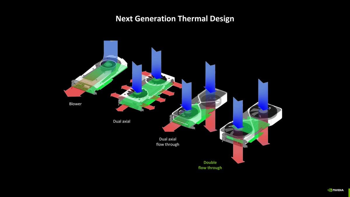
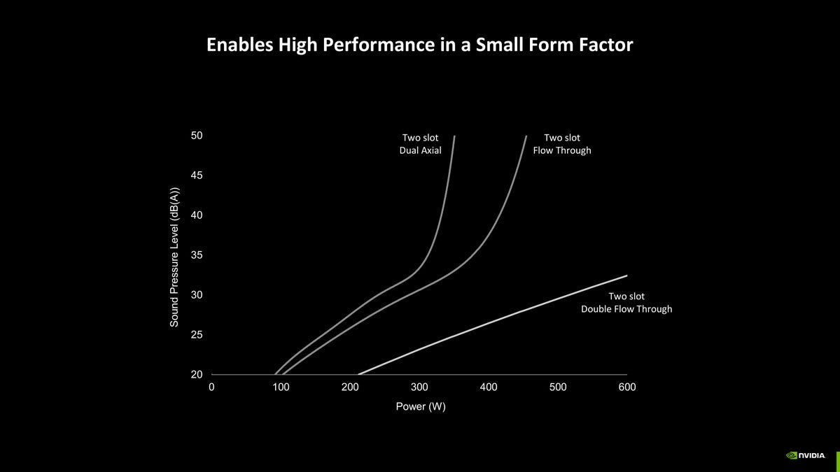
Thermal management typically relies on forced convection using air cooling with fans. However, as AI data centers increasingly transition toward liquid cooling solutions, it has become essential to rethink and enhance the thermal management strategies for advanced chips. This article will begin by examining the various chip-level cooling approaches, setting the stage for a deeper discussion on how to optimize thermal performance in this new era of high-power AI computing.
The fundamental mechanisms of heat transfer in chips include conduction, convection, and radiation. However, due to practical limitations such as package size, material thermal conductivity, and heat diffusion path length, effective thermal management in real-world applications primarily relies on conduction and convection.
In high-performance logic chips and AI accelerators, efficiently transferring the heat generated at the chip’s core to the package surface—where it can be removed by a cooling solution—is essential for ensuring system stability and extending operational lifespan.

For TSMC, the challenge of chip thermal management is not only tied to process node scaling but also critically impacts the competitiveness of its advanced packaging technologies—such as CoWoS and SoIC—in the high-end AI and HPC markets. As customer demand for large die sizes and high-bandwidth memory integration continues to grow, TSMC is actively refining its technology roadmap to address these trends.

Entering the N2 era, TSMC has officially transitioned from traditional FinFET structures to the Gate-All-Around (GAA) Nanosheet architecture. This shift not only improves transistor electrostatic control and density but also offers potential thermal advantages. The GAA structure enables the transistor channels to be distributed more evenly in three-dimensional space, allowing for better thermal distribution and reducing the risk of localized overheating. Additionally, TSMC’s N2 node introduces a “dual track” standard cell design, enabling customers to choose between different performance and density trade-offs based on application needs, further balancing thermal density and performance.

Under this architecture, TSMC’s process roadmap can be broadly divided into two paths: one without backside power delivery technology (Super Power Rail, SPR), evolving from N2 to A14 and A10, focusing on pure CMOS scaling; and the other integrating SPR technology, advancing from A16 to A12, specifically targeting high-performance and high-power-density applications. Notably, TSMC has also introduced an A14P (Performance Enhanced) variant at the A14 node, which incorporates partial SPR elements to improve power delivery and thermal conduction efficiency as a transitional solution before fully adopting SPR.

However, overcoming thermal challenges cannot rely solely on transistor architecture and power delivery innovations. On the packaging level, backside grinding of the silicon die has long been a standard process to reduce chip thickness and shorten the thermal diffusion path, thereby improving thermal conduction. Nevertheless, excessive thinning can compress the thermal budget, potentially compromising package reliability and process stability. This makes Thermal Interface Materials (TIMs) a critical element in the thermal management strategy.
Henkel’s Comprehensive Positioning in Advanced Packaging Materials
Henkel is a highly capable player in the semiconductor materials space, with a comprehensive portfolio for Advanced Packaging, particularly in Heterogeneous Integration (HI) and High-Performance Computing (HPC). Henkel’s materials and technologies span the entire semiconductor value chain, from wafer manufacturing and packaging to module and system integration. Henkel emphasizes:
Thermo-mechanical stress management for 2.5D/3D ICs and large packages (>80x80mm).
Addressing the increasing power and thermal challenges driven by AI and HPC workloads with next-generation materials.
Offering Liquid Compression Molding (LCM), Lid/Stiffener Attach Adhesives, and Capillary Underfill as part of a full-spectrum materials solution.
Henkel’s TIM and Molding Solutions
High-Performance TIM and Molding Technologies
Liquid Compression Molding (LCM):
Ultra-Low Warpage: Ideal for WLP, PLP, and 2.5D/3D ICs.
Void-Free Gap Filling: Supports ultra-thin gaps below 20μm.
Environmentally Compliant: PFAS-Free and CMR-Free, promoting sustainability.
High Reliability: MSL1 and TCB > 1000x, suitable for high-reliability applications.
Applicable for wafer-level and chip-level underfill and gap-filling processes.
Lid / Stiffener Attach Adhesives:
Available in conductive and non-conductive versions, designed to enhance coplanarity and reliability for large-format packages (>80x80mm).
Provides high toughness, excellent adhesion, and low stress, suitable for complex package structures.
Capillary Underfill:
Fast flow and long workability window (over 20% flow improvement).
Void-free filling capability.
Improved crack resistance and low Coefficient of Thermal Expansion (CTE), supporting large bare die packaging.
Henkel’s Advanced Packaging Application Coverage
Supported Packaging Types and Applications
2.5D/3D ICs: Enabling warpage control and gap filling for large, multi-die stacks.
Fan-Out/Wafer-Level Packaging: Offering complete solutions for warpage control and chemical stabilityduring RDL processing.
High-Density HBM Memory Packaging: Addressing stress and gap-filling challenges in HBM stacking.
AI/HPC Server and Data Center Chips: Optimizing thermal management and enhancing large-package reliability.
Key Use Cases
High thermal conductivity TIM for CPU/GPU and AI accelerator packaging.
Low-stress underfill and molding for HPC, 5G, and networking chips.
Lid/Stiffener attach and warpage control for large package modules such as CoWoS, I-Cube, and X-Cube.
Thermal management for Fan-Out packaging in consumer electronics like smartphones and laptops.

Currently, the TIM solutions adopted in TSMC’s advanced packaging include high-thermal-conductivity polymers, silicon oxide (SiOx) thin films, and more advanced liquid metal TIMs. These materials are designed to minimize thermal resistance between the die and the package, enhancing the efficiency of the thermal conduction path. This becomes especially critical in advanced 3D heterogeneous integration packages such as SoIC-X, where vertically stacked die structures introduce unprecedented thermal density challenges. In these scenarios, the use of high-performance TIMs is essential to ensure system stability.
In summary, chip thermal design is evolving from a task of simple material selection and packaging optimization into a system-level co-design challenge. TSMC, through its deployment of GAA architecture, dual track standard cell design, backside power delivery (SPR), and diversified TIM material strategies, demonstrates forward-looking leadership in integrating process and thermal co-optimization. Looking ahead, as AI chips push power consumption toward the 2–3 kW range, thermal management capabilities will increasingly define the competitive threshold for foundries in both advanced process nodes and heterogeneous integration markets.

Bolt-on cooler. This is the current state-of-the-art in data centers. A cold plate sits on top of the lid instead of a heatsink. TIMs are used above and below.
Directly bonded cooler. This configuration is beginning to be adopted in some places. The cooler is directly bonded to the chip, with only one layer of thermal interface material. Imec’s prototype uses this layout, with modifications.
Backside cooling. Only presented in research, this layout allows the coolant to be closer to the heat source. Instead of bonding, it uses a dielectric liquid that makes direct contact to the chip. Because there is a vertical connection between the liquid and the chip, it avoids the thermal gradient problems of a lateral design.
In-chip cooling. This is the idea that Corintis is trying to commercialize. The coolant is contained within channels embedded in the chip. While it can offer optimal cooling, one potential challenge is that there may not be enough space for channels at lower pitches.
For Paid Members, SemiVision will discuss topics on
2025 Intel Foundry Direct Connect event
Liquid Metal TIM: Enhancing Thermal Conductivity
In-Package Liquid Cooling: Integrated Thermal Design
Superfluid Immersion Liquid Cooling: Preparing for Future Ultra-High Power Demands
The Expanding Role of Foundries: From Process Provider to System Integrator
TSMC’s TIM Technology Choices and Applications
Thermal Conductivity and Material Selection Criteria
Thermal Resistance and Contact Resistance
Directional Heat Transfer Considerations in Material Selection
Practical Challenges and Process Control in TIM Application
Practical Challenges and Process Control in TIM Application
What Is Microfluidic Channel Cooling?
TSMC’s Pathfinding Strategy: MEMS-Based Microfluidic Integration
Integration Challenges: TSV and DRIE
Packaging Integration and Application Potential
Cross-Layer Co-Design: From Materials to Systems
Outlook: Toward 2kW-Class AI/HPC Chip Cooling
Intel’s Thermal Innovations Highlighted at the 2025 Foundry Direct Connect Event
Beyond In-Package Liquid Cooling: Intel’s Superfluid Immersion Cooling
Global TIM Market and Supply Chain Analysis
Market Distribution and Application Examples
Thermal Management and TIM Applications in Advanced Packaging Technologies
OSAT Contributions and TIM Innovations