


Bridging Silicon, Systems and Society: The EPS Mission
Original Article by SemiVision (IEEE EPS , IEEE ECTC ,Unimicron)


Introduction to the IEEE Electronics Packaging Society (EPS)

Mission and Scope
The IEEE Electronics Packaging Society (EPS) is a globally recognized professional society under IEEE, dedicated to advancing technologies in electronics and microsystems packaging and manufacturing. EPS serves as a key platform for scientists and engineers to engage in the exchange of knowledge spanning research, design, and development. Its mission is to promote the advancement of electrical and electronic engineering through technical meetings, peer-reviewed journals, and publications that foster collaboration and knowledge sharing among members.
Historical Background
1950s Origin: The roots of EPS date back to 1950, when several U.S. organizations co-hosted the “Symposium on Improving Component Reliability,” which later evolved into the IRE Professional Group on Components and Materials—eventually becoming the IEEE CPMT Society.
2000: The CPMT Society celebrated its 50th anniversary with a historical retrospective.
2017: The society was officially renamed to IEEE Electronics Packaging Society (EPS) to better reflect its focus and mission in the electronics packaging field.
Technical Scope and Committees
EPS covers a broad range of applications related to materials, components, modules, and heterogeneous systems in electronic packaging. Key areas include modeling, processing, interconnects, thermal management, and reliability.
The society is structured into several technical committees, which regularly organize webinars and publish technical content. Focus areas include:
3D/TSV Integration
Electrical Design and Simulation
Advanced Materials
Thermo-mechanical Engineering
Reliability
RF & High-Speed Design
Photonics
Testing
Power Electronics
Publications and Conferences
EPS publishes a range of peer-reviewed journals, including the flagship IEEE Transactions on Components, Packaging and Manufacturing Technology (T-CPMT). It also organizes and sponsors numerous leading international conferences such as:
IMPACT (International Microsystems, Packaging, Assembly and Circuits Technology Conference)
EPEPS (Electrical Performance of Electronic Packaging and Systems)
3D-PEIM, MID Congress, PAINE, among others
These events serve as critical venues for presenting the latest innovations and fostering industry-academic collaboration.
Governance and Chapter Structure
EPS is governed by an elected Board of Governors, including the president, vice presidents, and program directors. It operates under formal documents such as the Bylaws, Operations Manual, and Strategic Plan.
The society has over 30 regional chapters worldwide—including in Taiwan, Europe, and North America—as well as student branches to encourage undergraduate and graduate student engagement in technical talks and project-based learning.
Awards and Distinguished Members
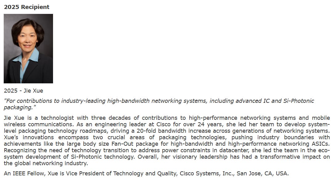
EPS has established several awards to honor outstanding contributions in the field of electronics packaging. One of its most prestigious recognitions is the IEEE Rao R. Tummala Electronics Packaging Award, established by the IEEE Board of Directors in 2002, which recognizes excellence in research and manufacturing technologies.

The 2025 recipient is Jie Xue, recognized for his pioneering work in high-frequency network systems and photonic packaging.
Membership and Professional Development
EPS offers various membership types, including professional, student, and project-based participation. Members gain access to:
Cutting-edge technical news
Online webinars
Career development resources
EPS also provides:
Certification programs
The Distinguished Lecturer Program
Scholarships and mentorship resources
These initiatives help members enhance both their technical expertise and leadership capabilities.


The IEEE Electronics Packaging Society (EPS) is a cornerstone organization in the global electronics and microsystems packaging ecosystem. It not only delivers high-quality conferences and peer-reviewed publications but also provides a wealth of resources and professional development opportunities for its members.
With a robust structure of technical committees and global chapters, EPS plays a pivotal role in driving innovation and advancing the frontiers of packaging technology.
For more information on EPS’s focus areas, upcoming conferences, or membership details, please visit the official IEEE EPS website and explore the technical committee pages.Special Lecture on Silicon Photonics and CPO
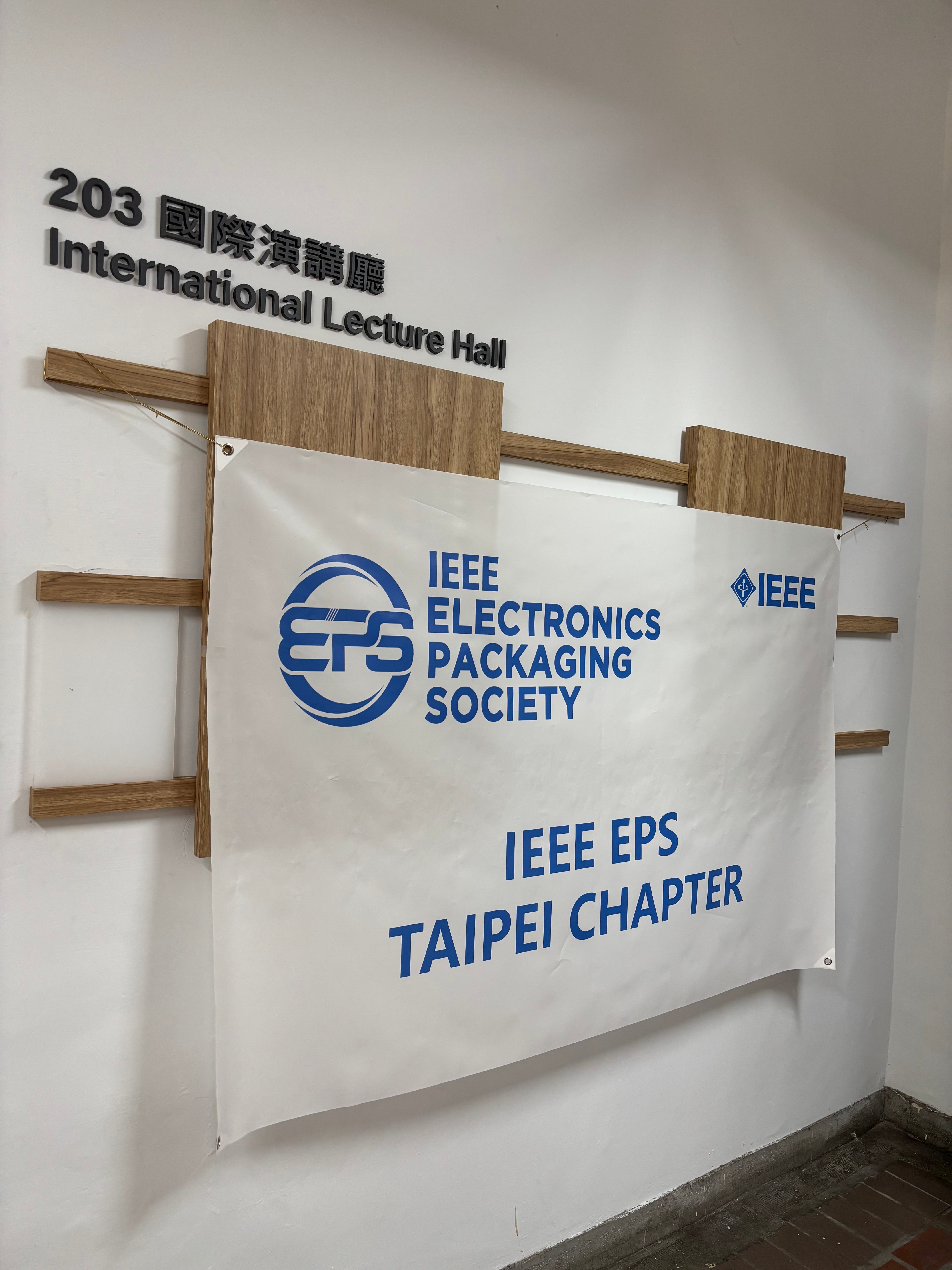
We would also like to extend our appreciation to IEEE EPS Taiwan Chapter for playing a crucial role in supporting the event. EPS continues to be a vital force in advancing packaging technologies within Taiwan and across the globe.
About IEEE Electronics Packaging Society (EPS)
The IEEE Electronics Packaging Society (EPS) is the world’s leading professional organization dedicated to advanced packaging, heterogeneous integration, microsystems technologies, and cross-disciplinary applications. EPS covers a comprehensive range of topics—from materials and processes, simulation and modeling, high-density substrates, and thermal-mechanical design to photonic packaging, RF, and reliability testing—supporting the electronics industry from silicon to system.
Core Mission and Structure
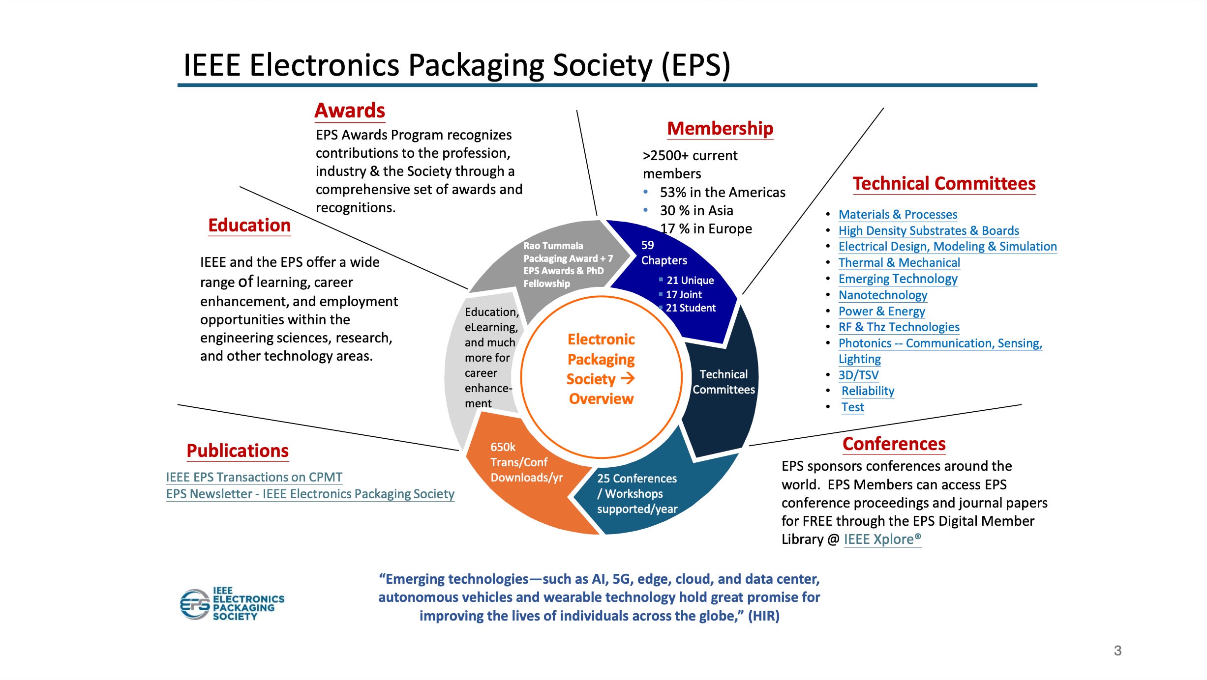
EPS drives industry-academic collaboration through five key pillars:
Technical Committees
Publications
Education
Awards
Conferences and Forums
Its technical committees cover a wide array of domains including materials and processes, 3D packaging/TSV, electrical and thermal simulation, nanotechnology, power and energy systems, RF and THz technologies, photonic communications and lighting, and reliability and testing.
EPS publishes journals such as the IEEE Transactions on Components, Packaging and Manufacturing Technology (T‑CPMT) and the EPS Newsletter, both freely accessible to members.
In education, EPS focuses on reskilling engineers, supporting career development, and enabling industry transformation through resources integrated with IEEE Xplore, including access to conference proceedings and journal papers.
EPS boasts over 2,500 professional members worldwide, with 53% from the Americas, 30% from Asia, and 17% from Europe, and supports over 25 major international conferences each year through a network of 59 chapters globally.
EPS Distinguished Lecturer Program
Currently, 34 internationally recognized experts participate in the EPS Distinguished Lecturer Program. These speakers cover all major areas of electronics packaging and regularly deliver lectures at leading universities, research institutions, and industry conferences around the world, actively promoting global knowledge exchange and technical outreach.
Global Presence and Technical Communities
EPS has established over 40 local and joint chapters across 10 major global regions, supporting a broad and diverse technical community. The regional distribution is as follows:
North America (Regions 1–7): Hosts the most concentrated technical communities, particularly in Silicon Valley and the U.S. East Coast.
Asia (Region 10): Chapters are rapidly expanding in high-tech regions such as Taiwan, Japan, South Korea, China, Singapore, India, and Vietnam.
Europe (Region 8): Key locations include Germany, Switzerland, the United Kingdom, France, and Italy.

Through its global chapter network, EPS actively organizes both in-person and virtual seminars, technical forums, and talent development programs, strengthening the connection between academia, research, and industry across regions.
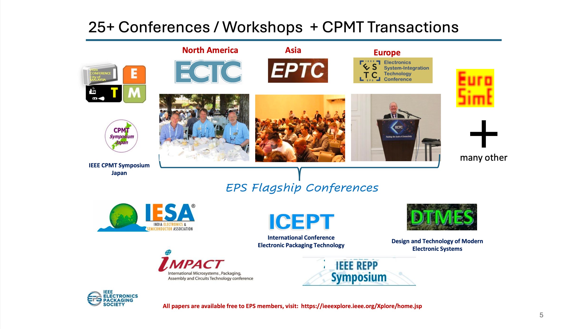
EPS-Sponsored International Conferences and Technical Platforms
Each year, the IEEE Electronics Packaging Society (EPS) supports over 25 professional international conferences and workshops across the Americas, Asia, and Europe, forming one of the most influential global networks in the electronic packaging field. Key conferences include:
North America:
ECTC (Electronics Components and Technology Conference)
IEEE CPMT Symposium (Japan/Malaysia)
Asia:
EPTC (Electronic Packaging Technology Conference, Singapore)
ICEPT (International Conference on Electronic Packaging Technology, China)
Europe:
ESTC (Electronics System-Integration Technology Conference)
EuroSimE (focused on thermal-mechanical engineering and reliability)
Other notable conferences include IMPACT (Taiwan), DTMES (India), and IEEE REPP, with free access to conference papers and technical materials available to EPS members via the IEEE Xplore platform.
Community Mission and Industry Impact
EPS is committed to advancing the practical adoption of heterogeneous integration and advanced packaging technologies through focused efforts in the following strategic areas:
AI and Data Center Architecture Transformation (AI, HPC, 5G, edge/cloud)
Automotive Electronics: addressing challenges in thermal reliability, modular design, and ruggedized packaging
Wearables and Consumer Devices: enabling high-density system integration
Low-Power, High-Bandwidth Interconnects: innovation in materials and advanced packaging structures
“Packaging is Platform”: the forward-looking design philosophy driving system-level integration
Through its technical committees, industry white papers, certification programs, and conference platforms, EPS is leading the global electronics packaging community toward a new era of heterogeneous and system-level innovation.
A Platform for Innovation Across Academia, Industry, and Education
The IEEE Electronics Packaging Society (EPS) is more than a technical society—it is a global platform bridging academia, industry, and education in the field of electronic packaging. From curated educational resources and top-tier conferences to innovation in materials and integration technologies, EPS provides a comprehensive and continuously evolving knowledge and collaboration ecosystem.
For engineers, researchers, and industry decision-makers, joining EPS means stepping to the forefront of packaging technology and collaborating with the world’s leading experts to shape the future of electronics.
To learn more or apply for membership, please visit:
👉 https://eps.ieee.org
The recent seminar was organized by Professor Jhen-Hong Gau of the Department of Materials Science and Engineering at National Taiwan University, who invited Dr. John Lau to deliver a specialized talk on Co-Packaged Optics (CPO). The event focused on Silicon Photonics, CPO technologies, and related R&D projects, offering in-depth insights and engaging discussion. Jun.18, 2025
Dr. John H. Lau, Ph.D., P.E. is a globally recognized authority in advanced semiconductor packaging, with over 40 years of R&D and manufacturing experience in areas such as system-in-package (SiP), fan-in/out wafer-level packaging, 2D–3D IC integration, chiplet heterogeneous integration, and thermal/reliability engineering .
Professional Career & Leadership
Served nearly 25 years at Hewlett-Packard/Agilent Labs in Palo Alto, pioneering new packaging processes .
Held leadership roles including Director at the Institute of Microelectronics (Singapore), Specialist at ITRI (Taiwan), and Senior Technical Advisor at ASM Pacific Technology (Hong Kong) .
Since 2019, held key positions at Unimicron Technology (Taiwan), including CTO and ongoing senior advisory roles .
Technical & Scholarly Impact
Authored or co-authored 23 textbooks, including Semiconductor Advanced Packaging (Springer 2021), Chiplet Design and Heterogeneous Integration Packaging (2023), and works on flip‑chip and hybrid bonding .
Published over 520 peer‑reviewed papers and holds 50+ U.S. patents, driving innovation in thermocompression/hybrid bonding, interposer design, and dielectric materials for high-speed applications .
Industry Influence & Recognition
Elected Fellow of IEEE, ASME, and IMAPS, recipients of prestigious awards such as IEEE CPMT Field Award and ASME Worcester Reed Warner Medal .
Frequently invited as a keynote speaker and instructor at leading forums (e.g., ECTC, IEEE CPCMT, SEMICON), shaping industry standards and training engineers in advanced packaging methodologies .
Key Technical Contributions
Pioneered packaging evolutions from traditional 2D through 2.5D/3D IC, championing fan-in/out WLP, TSV-less interposers, and hybrid bonding approaches .
Advanced chiplet-scale heterogeneous integration, crucial for scalable, high-performance multi-die systems in AI accelerators and co-packaged optics .
Led development in reliability engineering, with extensive work on solder joint robustness, thermal cycling resilience, and low-loss packaging materials ideal for high-frequency operations .
Dr. John H. Lau’s unparalleled breadth of experience, from academia to industry leadership, coupled with his scholarly contributions and patented innovations, makes him a pioneering force in advanced semiconductor packaging. His work continues to lay the foundations for modern heterogeneous integration, chiplet architectures, and Next‑Gen packaging technologies driving the semiconductor industry forward.

For Paid Members, SemiVision will discuss topics on
Co-Packaged Optics (CPO): Technology Integration, Industry Landscape, and Future Outlook
Definition, Value, and Fundamental Distinction Between Co-Packaged Optics (CPO) and Silicon Photonics (SiPh)
Target Applications and Market Positioning
Heterogeneous Integration of PIC and EIC
Key Interconnect Technologies in Advanced Packaging
Representative Companies and Technology Implementations (Intel ,Cisco ,SPIL , AMD ,TSMC , Apple)
Academic and Industrial Collaboration Platforms
Technology Insights and Industry Updates
CPO as the Optical Interconnect Breakthrough