Chips in the Age of Intelligence: How AI and LLMs Are Reshaping Design and Manufacturing
Original Article by SemiVision Research
The global semiconductor chip war has reached a fever pitch—semiconductors are no longer just a part of the tech industry, but have become strategic assets that nations are fiercely competing over. The convergence of U.S.-China tech tensions, the rise of AI applications, and the reorganization of global supply chains has elevated chip design and manufacturing from purely technical issues to core matters of national security and economic sovereignty.
Amid this competitive wave, Taiwan—represented by TSMC’s dominant foundry capabilities—continues to hold the global lead. However, challenges are emerging from multiple fronts: China’s push for domestic alternatives, U.S. onshoring initiatives such as the CHIPS Act, and the growing trend of cloud service providers (CSPs) designing custom ASICs. Recently, the U.S. government restricted exports of NVIDIA’s H20 and certain high-end gaming GPUs to China, a move aimed at slowing China’s progress in AI chip development. Yet, China’s advancements—evident in Huawei’s Ascend chip architecture and the Deepseek AI models—signal a strong undercurrent of demand and technological momentum that cannot be underestimated.
For Taiwan to maintain its critical position in this global race, it must evolve beyond manufacturing excellence and move into chip design, advanced packaging, and system-level platform integration—forming a complete and irreplaceable “Silicon Island Chain.” From the perspective of future chip design, ASICs (Application-Specific Integrated Circuits) are rapidly replacing general-purpose processors as the mainstream due to the extreme performance and energy-efficiency demands of large-scale AI models, 5G communications, and data center computing. Traditional CPU and GPU architectures struggle to keep up with evolving algorithms and workload dynamics.
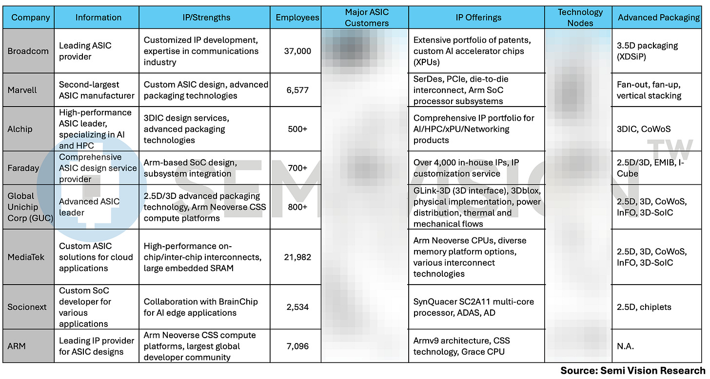
In response, major CSPs like Google, AWS, Meta, and Microsoft have developed in-house AI accelerators and data center chips—TPU, Graviton, Trainium, Cobalt, and MTIA, among others. These chips represent the next generation of cloud infrastructure and are reshaping the dynamics of IC design and manufacturing. Broadcom stands out as a leading ASIC service provider. Unlike others, Broadcom does not emphasize its own brand but instead delivers deeply customized ASIC design services to enterprise clients. Their expertise spans high-speed SerDes, networking protocols, packet processing, and AI acceleration, serving clients such as Google, AWS, Meta, VMware, and Cisco. This business model—marked by high technical barriers, long-term client engagement, and stable margins—serves as a valuable reference for Taiwanese firms aspiring to enter high-end B2B design services.
For more in-depth discussion on this topic, please refer to previous articles published by SemiVision.
Taiwan hosts several leading companies providing ASIC (Application-Specific Integrated Circuit) design and turnkey services, especially for AI, HPC, communications, and edge applications. The key players include:
GUC (Global Unichip Corp.) – A close TSMC partner, offering advanced-node ASIC design, chiplet integration, and backend implementation services, widely adopted in HPC and AI markets.
MediaTek (MTK) – In addition to its mainstream SoC products, MediaTek has developed custom ASIC and AI solutions for strategic partners and hyperscale customers.
Aichip Technologies – A rising design house providing full-stack ASIC design services targeting AI workloads and ultra-low power applications.
Faraday Technology – A veteran IP and ASIC service provider, offering a broad portfolio of silicon-proven IP and turnkey SoC services, particularly strong in mature and mixed-signal nodes.
Together, these companies form the core of Taiwan’s ASIC ecosystem, bridging advanced foundry technologies with customized silicon solutions to meet the diverse demands of global semiconductor innovation.
In Taiwan, the most promising opportunity lies in deep strategic collaboration between TSMC and MediaTek, further bolstered by partnerships with AI giants like NVIDIA. Together, they can drive a comprehensive flow from chip design and advanced packaging to platform module development and simulation validation. TSMC’s packaging technologies—such as CoWoS, SoIC, and Chip-on-Wafer—paired with UCIe standards, are paving the way for future chiplet architectures. Meanwhile, MediaTek’s expertise in AP and modem design, if extended to areas like industrial control, edge AI, and automotive electronics, could unlock entirely new markets.
Looking ahead, three key trends will define the future of chip design:
Chiplet-based modular architectures will reduce development costs and increase design flexibility. With UCIe and similar interconnect standards, multi-vendor and cross-node system integration will become possible.
Optical I/O integration in chip design and packaging will address the Tbps-level bandwidth and latency challenges in AI clusters, evolving alongside CPO and LPO technologies.
Design automation and generative IC design tools will become mainstream in EDA workflows. AI-assisted tools will optimize circuit performance, layout, and power analysis, drastically shortening design cycles.
These trends will feed back into process node selection, packaging strategies, and testing methodologies—driving a full-scale upgrade and vertical integration of Taiwan’s semiconductor supply chain. In this context, chip design is no longer a siloed in-house effort, but a critical node of cross-company and cross-regional collaboration. If Taiwan can find leverage points among chip design, packaging, and platform integration, it stands a strong chance of maintaining its pivotal role in the global semiconductor strategy.
SemiVision will continue tracking developments in CSP in-house chip design, AI chip packaging platforms, and Taiwan’s efforts to build a next-generation chip design ecosystem through institutional innovation and industrial collaboration—providing readers with frontline insights and deep analysis.
For Paid Members , SemiVision will discuss topics on
Status of Deepseek updated
Exploring in LLM Scaling and AI Applications
Application Scenarios Are Shaping the Future of Chip Design
How Chip Design Trends Are Reshaping Semiconductor Manufacturing
The Future of Chips: Smarter Brains & Broader Applications
Chip Design Trends: The New Priorities in Semiconductor Manufacturing


