Dual Engines of Technology and Capacity: Ajinomoto’s Strategic Ascent in the Advanced Substrate Market
Original Articles By SemiVision Research (IEEE ECTC , Ajinomoto , TSMC ,Nvidia)
As artificial intelligence (AI) and high-performance computing (HPC) advance at breakneck speed, chip packaging is evolving toward unprecedented scale and complexity. Packaging modules have expanded rapidly from the 75mm class to over 120mm, with layer counts exceeding 20. This not only signifies greater computational density but also brings more severe manufacturing challenges and yield pressures. In this wave of packaging evolution, the role of build-up substrates has become increasingly critical—especially within 2.5D heterogeneous integration platforms like TSMC’s CoWoS®. As the structural backbone between logic chips and memory, substrates must endure not only electrical demands but also thermal, mechanical, and material stresses.
ABF-GCP has emerged as a next-generation substrate material gaining industry-wide attention. By incorporating reinforced glass cloth and primer layers into the ABF structure, this composite design enhances dimensional stability and has been repeatedly demonstrated to suppress crack propagation and absorb mechanical stress. Even without a stiffener, it maintains structural integrity under high-temperature reflow conditions (up to 250°C), significantly mitigating “smiley face” warpage and offering robust support during backend wafer packaging processes.
However, warpage control is not merely a materials science issue—it also involves system-level design. While introducing a stiffener can help manage overall deformation, mismatches in the coefficient of thermal expansion (CTE) between the stiffener, resin, and ABF layers can actually induce cracks. This has ushered in a new era of “CTE co-design,” emphasizing the need to coordinate thermal-mechanical behavior across multiple materials to reduce failure risks from the ground up.
As the application of ABF-GCP expands in large-scale, high I/O packaging, supply chain stability is drawing increased scrutiny. In 2025, Nittobo announced a 20% price hike for advanced glass fibers, underscoring the real-world challenges of securing materials for advanced packaging. In the balancing act between material innovation and scalable production, identifying alternatives, diversifying suppliers, and building robust material verification platforms are becoming essential strategies for enhancing industry resilience.
From Umami to Advanced Packaging: How Ajinomoto is Leading the Materials Revolution in Semiconductor Substrates
With the rapid rise of AI and high-performance computing (HPC), chip packaging is evolving into a new era of ultra-high density and large-scale modules. At the heart of this transformation is Ajinomoto Build-up Film (ABF), a critical material enabling advanced semiconductor integration. Behind this material is Ajinomoto—a company once known solely for seasoning, now an invisible giant shaping the future of electronic materials.
1. From Seasoning to Semiconductor Powerhouse
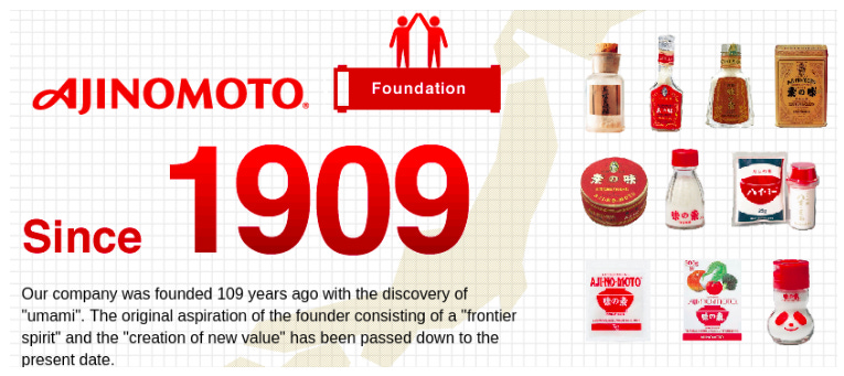
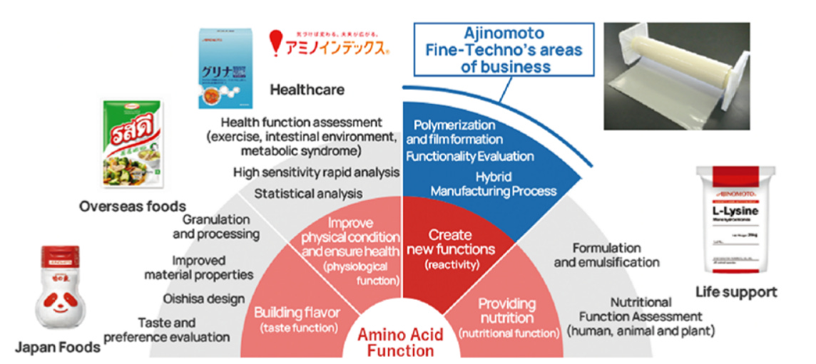
Founded in 1909, Ajinomoto Co., Inc. began with food products and amino acid research. Over the decades, it expanded into biotechnology and advanced materials. Its subsidiary, Ajinomoto Fine-Techno, launched ABF materials in the late 1990s. Since then, ABF has become the de facto industry standard for CPU and GPU packaging, commanding a market share of over 95%.
ABF is a thermosetting composite film that blends organic resin and inorganic fillers. It offers excellent thermal stability and dimensional control, making it ideal for fine-pitch multilayer structures and high-density redistribution layers used in 2.5D and 3D packaging.
2. ABF: A Cornerstone of Advanced Substrate Technology
ABF materials exhibit ultra-low Coefficient of Thermal Expansion (CTE), high heat resistance, and excellent electrical insulation, enabling them to withstand multiple reflows and complex stacking. ABF is widely adopted for:
CoWoS®, EMIB, and chiplet-based heterogeneous integration
High-I/O, high-frequency applications (e.g., AI accelerators and high-speed SerDes)
Multi-layer RDL (redistribution layer) substrates in CPU/GPU packaging
Ajinomoto continues to develop next-generation ABF variants with lower dielectric constants and reduced CTE to enhance reliability in high-temperature and high-frequency environments. The company presented multiple papers at the 2025 IEEE ECTC, demonstrating its latest achievements in warpage control, stress absorption, and material synergy.
3. Strategic Expansion and Platform Integration
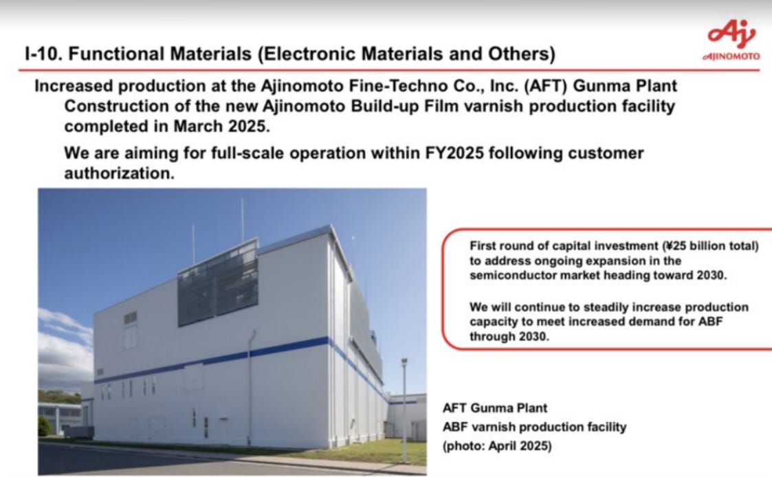
To meet surging demand, Ajinomoto is investing in production capacity at its Gunma and Kawasaki plants in Japan. By 2030, it aims to increase output by over 50%. This strategic move supports the company’s rapidly growing electronic materials business and reinforces its ties with major chipmakers and OSATs (e.g., TSMC, Intel, Samsung).
Ajinomoto is also deeply engaged in co-developing solutions with advanced packaging platforms. It emphasizes “CTE-coordinated design,” optimizing the thermal-mechanical behavior of multi-material stacks (ABF, resin, stiffeners) to prevent warpage and cracking—especially crucial in large, high-layer substrates.
4. Outlook: From Materials to Strategic Integration
Innovative materials like ABF-GCP are not merely incremental upgrades—they are essential enablers of yield, reliability, and performance in large-package manufacturing. Leveraging its deep expertise in polymer chemistry and amino acid-based materials science, Ajinomoto is ushering in a new era of science-driven materials innovation.
Despite cost pressures and supply chain risks—such as Nittobo’s 2025 announcement of a 20% price hike for high-end fiberglass—Ajinomoto has diversified its supplier base and developed robust multi-material strategies to maintain resilience and scalability.
Ajinomoto’s packaging strategy is no longer just about materials supply—it is about co-designing the future of advanced semiconductor systems. As chips grow in size and complexity, ABF and its evolving derivatives will remain a foundational enabler of next-generation packaging solutions, offering a reliable bridge between silicon and system integration.
For Paid Members, SemiVision will discuss topics on
Brief Introduction to Advance Package Roadmap and Substate
Advanced Package Classification and CoWoS Material Overview
What is a Build-up Substrate?
Core Material Selection ( Organic Core & Glass Core)
Build-up Layers (BU Layers) Study
Build-up Film Material Study and Supply Chain Analysis
Introduction to ABF-related concepts
Ajinomoto’s Experimental Section
Ajinomoto’s Experimental Details Discussion
Ajinomoto’s Substrate Configuration
Ajinomoto’s Substrate Configuration
Thermal Cycling and Thermal Load Testing
Thermal Cycling Test After UF Filling
Warpage measured using the shadow moiré method after 1500 TCT (Thermal Cycling Test) cycles.
Thermal Cycling Test After Stiffener Attachment
Crack Propagation Comparison
The application of Glass fiber from Nittobo’s key presentation
Key observations from the trend from Nittobo’s Viewpoint


