From Barrier-Limited to Barrier-Free: IBM’s New Blueprint for BEOL Scaling
Original Articles by SemiVision Research (IEEE IITC , IBM , TSMC , UMC , Global Foundry , Imec , Intel , NYCU )


As advanced logic process nodes push toward 2nm and beyond, traditional copper (Cu) interconnect technologies are facing significant challenges. These include sharply rising resistance due to line width scaling, declining reliability, and increasing parasitic impact from the proportion of barrier and liner layers. In response to these bottlenecks, IBM presented a pivotal technical paper at the 2025 IEEE International Interconnect Technology Conference (IITC), titled
“Innovations Enabling the Continued Extendibility of Cu and Post-Cu Damascene BEOL Technology.”
The paper introduces a comprehensive suite of innovations aimed at extending the viability of BEOL (Back-End-of-Line) scaling.
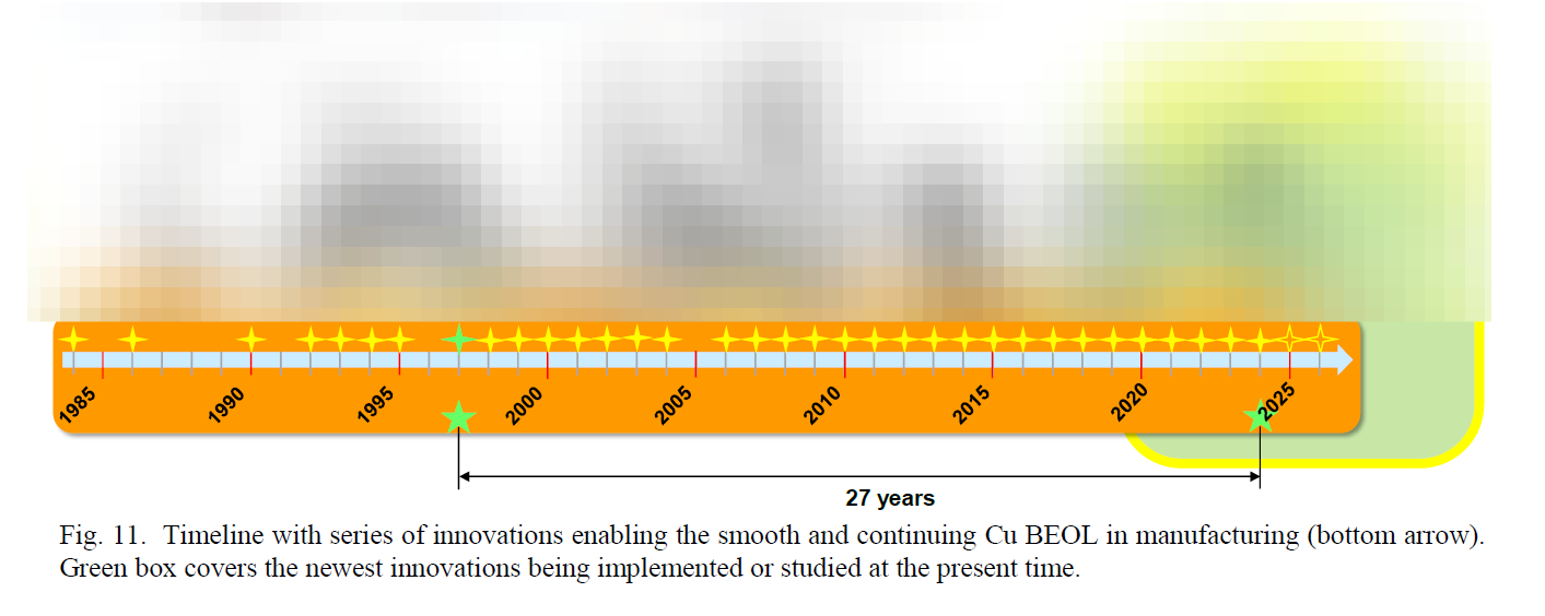
This work not only reviews nearly three decades of evolution in Cu Damascene processing, but also unveils IBM’s latest breakthroughs across materials, structures, and process integration. Key highlights include a next-generation low-k dielectric (ALK), full hardmask removal (FHMR), advanced Cu reflow metallization (Access-3 Reflow), and a Post-Cu alternative: Rhodium (Rh) Damascene integration. Notably, these innovations are designed to be integrated within existing BEOL frameworks, enabling logic chips to scale down toward 1.4nm nodes and beyond with validated reliability and manufacturability.
This report will provide a full analysis of the technical context, experimental results, and future outlook behind IBM’s research, and explore its broader implications for the evolution of BEOL interconnect technologies across the semiconductor industry.
About IITC: A Global Forum for Advanced Interconnect Technology
The IEEE International Interconnect Technology Conference (IITC) is one of the world’s most influential conferences dedicated to semiconductor back-end process and interconnect technologies. Since its inception in 1998, IITC has served as a leading platform for the innovation and exchange of ideas in chip interconnect structures, materials, and processing.
Organized by the IEEE Electron Devices Society, IITC focuses on key areas of Back-End-of-Line (BEOL) and Middle-of-Line (MOL) integration, covering a wide range of topics such as:
Metallization and barrier layer materials
Low-k and advanced dielectric integration
Reliability and electromigration
RC delay modeling and optimization
CMP (Chemical Mechanical Planarization) techniques
3D IC integration, Through-Silicon Vias (TSVs), and packaging interconnects
Emerging nanoscale and alternative interconnect architectures
The conference attracts participants from leading global semiconductor companies—including Intel, TSMC, Samsung—as well as integrated device manufacturers (IDMs), EDA vendors, material suppliers, academic institutions, and cutting-edge startups. Each year, IITC features keynote addresses and invited talks from industry and academic leaders, along with peer-reviewed technical papers showcasing the latest breakthroughs in interconnect research.
Beyond being an annual gathering for engineers and materials scientists, IITC has become a forward-looking forum that shapes the future of advanced logic node interconnect specifications and integration strategies. The insights shared at IITC directly influence decisions across the technology chain—from standard setting and EDA tool development to process integration and high-volume manufacturing deployment.
In an era where scaling and performance are increasingly defined by interconnect innovation, IITC remains a crucial window into the next-generation technologies that will power the semiconductor industry’s future.
IEEE International Interconnect Technology Conference (IITC) 2025 – Participants and Key Details
Conference Overview
The 2025 IEEE International Interconnect Technology Conference (IITC 2025) was held from June 2 to June 5 in Busan, South Korea, at the Westin Josun Hotel. It was hosted by the IEEE Electron Devices Society and co-organized with the Korean Institute of Electronic and Electrical Materials Engineers (KIEEME) and UNIST (Ulsan National Institute of Science and Technology). This marked the first time the conference was held in South Korea. The event focused on advanced interconnects, BEOL/MOL technologies, reliability, and integration solutions for sub-3nm logic nodes and heterogeneous systems.
Key Industry and Research Participants
IBM
Speaker: Dr. Daniel C. Edelstein
Presentation: “Innovations Enabling the Continued Extendibility of Cu and Post-Cu Damascene BEOL Technology”
Summary: IBM showcased new BEOL strategies involving low-k dielectrics (ALK), full hardmask removal (FHMR), Cu reflow (Access-3), and post-Cu alternatives such as Rhodium (Rh), designed to support scaling below 2nm with enhanced reliability and manufacturability.
imec (Belgium)
Participation: Presented 17 papers, including 14 as first author and 2 invited talks.
Lead Researchers: Giulio Marti, Blake Hodges, Zsolt Tokei
Topics: Advanced metallization schemes, electrical modeling, sub-2nm integration, and reliability-enhanced interconnect architectures.
Samsung Electronics
Speakers: Dr. Jong Myeong Lee, Dr. Kimin Jun
Topics: Advanced interconnect integration and bonding technologies for future semiconductor scaling.
SK hynix
Speaker: Dr. Jiho Kang
Presentation: “Semiconductor Technology Trends to Overcome Integration Limitations for Future AI Memory Devices”
Focus: Overcoming density and performance challenges in next-generation AI-oriented memory packaging.
Academic and Research Institutions
Tohoku University (Japan): Prof. Tetsu Tanaka
National Yang Ming Chiao Tung University (Taiwan): Prof. Jyehong Chen, Prof. Kuan-Neng Chen
National Sun Yat-sen University (Taiwan): Prof. Yung-Jr Hung
Pusan National University (Korea): Prof. Sehun Kwon
UNIST (Korea): Prof. Soo-Hyun Kim
Keio University (Japan): Dr. Munehiro Tada
imec (Belgium): Dr. Zsolt Tokei
Conference Highlights
Keynote sessions delivered by industry leaders on the future of logic scaling and interconnect innovation.
Technical sessions covered topics such as BEOL/MOL reliability, hybrid bonding, low-k integration, 3D packaging, and nanoscale metallization.
Poster sessions provided a platform for emerging researchers to showcase cutting-edge work and engage in international collaboration.

Since the late 20th century, IBM has been a pioneering force in advancing key semiconductor process technologies—particularly in the field of metal interconnects. In 1997, IBM became the first company to implement copper (Cu) Damascene interconnects at the 220nm technology node, breaking the industry’s long-standing reliance on aluminum (Al). Given copper’s lower resistivity and higher current-carrying capacity, this breakthrough significantly enhanced chip performance and reliability, laying a critical foundation for continued logic scaling in the years to follow.
However, the adoption of Cu interconnects was far from straightforward. Despite copper’s superior electrical properties, it could not be patterned using conventional dry etching techniques. This necessitated the development of a completely new Damascene process—where trenches were first etched into the dielectric and subsequently filled with metal. It also required the integration of effective barrier layers and low-k dielectric materials to prevent diffusion and ensure long-term reliability. IBM not only overcame these challenges but also succeeded in demonstrating volume manufacturability, making it the first company to commercialize Cu BEOL (Back-End-of-Line) technology. As a result, IBM is often regarded as the “originator of copper interconnect fabrication.”
Following IBM’s lead, the global foundry industry began to evaluate the viability of transitioning to copper. TSMC eventually introduced Cu interconnects at the 180nm node, complementing the shift with internally developed low-k materials and revamped process architecture. This enabled TSMC to rapidly complete the migration from Al to Cu and maintain its technology leadership. In contrast, UMC took a more conservative approach, delaying full Cu integration until the 130nm node. During that period, UMC continued to serve select customers using mature Al-based processes to balance performance stability with manufacturing cost-efficiency.

This chapter in semiconductor history not only underscores IBM’s leadership in materials science and process innovation but also highlights the divergent strategic decisions made by Taiwan’s two major foundries. Today, while IBM has transformed into a systems and R&D-centric company, its influence on BEOL technology development endures. Through continuous contributions to leading conferences such as IITC and IEDM, IBM remains a vital force shaping the future of semiconductor interconnect technology.

For Piad Members ,SemiVision will discuss topics on
Introduction of Copper Interconnects and Their Advantages
The Innovation of the Damascene Process
Challenges and Limitations in the Nanoscale Era
Industry Strategies to Extend Copper Viability
Key Takeaways from the BEOL Development Roadmap(ALK , ILD3.3 , FHMR , Access-3 Reflow , Innovation in Rh)
1. Next-Generation Low-k Material: ALK (Advanced low k material)
2. ILD3.3: An Advanced Inter-Layer Dielectric Balancing Reliability and Low RC Performance
3. FHMR (Full Hardmask Removal): A Breakthrough in Etch Mask Integration
4. Access-3 Reflow Process: Enabling Void-Free Cu Interconnects for Advanced Nodes
5. Post-Cu: Rhodium (Rh) Damascene Technology
Rh CMP (Chemical Mechanical Planarization): Challenges and Solutions
Performance Validation and Process Results
Industry Trend: The Deep Implications of “Shift to the Left”
Moving Away from Reactive Strategies
Building the Next-Generation BEOL Extendibility Platform
Summary of IBM’s Recent Technical Paper