

From Interconnect to Intelligence: Taiwan-Japan Driving the Future of Photonic Chiplets
Original Article by SemiVision Research (ASE , Foxconn, Suruga Seiki ,NTT ,TEEIA)

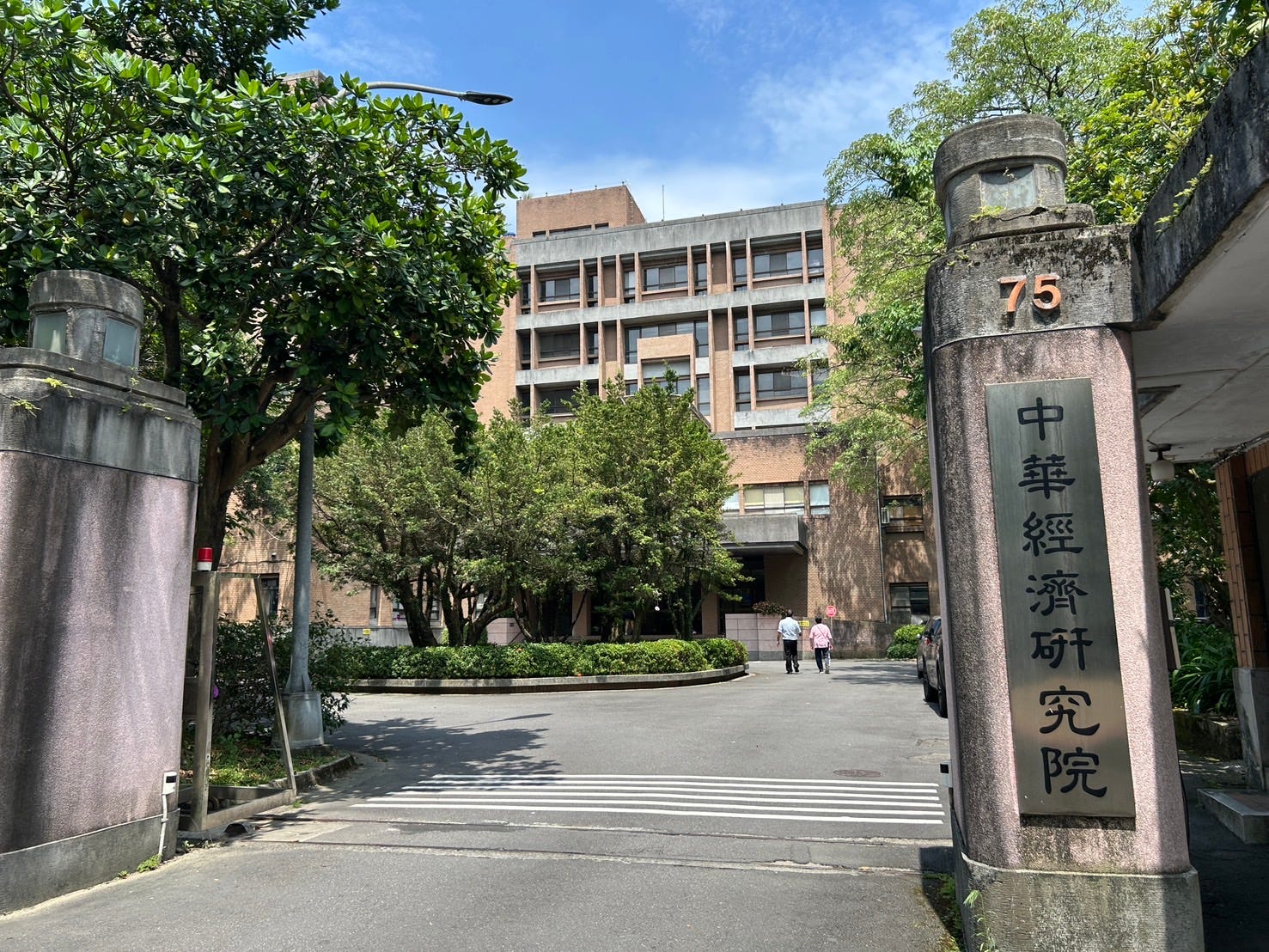
SemiVision was invited to participate in the Taiwan-Japan Semiconductor Technology Forum, hosted by the Department of Industrial Economics, Ministry of Economic Affairs, and co-organized by the Chung-Hua Institution for Economic Research.

IOWN: The Expansion and International Collaboration of Next-Generation Communication and Computing Infrastructure
Yosuke Aragane, Director, IOWN Promotion Office, Research Planning Division, Research and Development Planning Department, NTT

Session 1: Key Technologies and Global Deployment of Photonics-Electronics Convergence

Moderator: Prof. Hao-Chung Kuo, Chair Professor / Director, Department of Photonics, National Yang Ming Chiao Tung University / Semiconductor Research Institute, Foxconn Research Institute

Next-Generation Optical Communication Technology and International Standardization Strategy – Photonics-Electronics Convergence and AI
Hideki Isono, Representative, Former Senior Professional Engineer, Chair of IEC SC86C, Convener of SC86C WG4 / IGS Consulting / Fujitsu Optical Components Ltd. / IEC
Prospects for Taiwan-Japan Advanced Semiconductor Packaging Collaboration – The Case of Silicon Photonics
Alex Wu, President / Vice Chairman, Suruga Seiki Co., Ltd. Taiwan Branch / HiSPA – Heterogeneous Integration Silicon Photonics Alliance


Session 2: Building the Ecosystem for Heterogeneous Integration in Silicon Photonics
Moderator: Shinn-Yang Wang, Secretary General, Taiwan Electronic Equipment Industry Association (TEEIA)

Overview of AIST’s R&D on Photonics-Electronics Convergence
Takeru Amano, Director, Center for Photonics-Electronics Convergence, National Institute of Advanced Industrial Science and Technology (AIST)


Advanced Packaging Evaluation: Chiplet and Silicon Photonics-CPO
Vincent Lin, Director, Advanced Technology Development Division, ASE Group
Next-Generation Light Source Transmission Technology and Taiwan-Japan Collaborative Outlook
Evan Wu, General Manager, Ahead Photon Inc.

Session 3: Market Outlook of Underwater Communication Technologies
Moderator: Michel Chu, Partner, Acorn Campus Taiwan
Current Status and Future Outlook of Japan’s Underwater Optical Technologies
Takeshi Shimada, CEO, AQUADJUST Inc. / ALAN Alliance

Acoustic Monitoring and Long-Distance Communication Technologies in Taiwan’s Surrounding Seas
Linus Y.S. Chiu, Distinguished Professor and Director, Institute of Undersea Technology, National Sun Yat-sen University

In recent years, with the rapid advancement of Artificial Intelligence (AI) and Machine Learning (ML), the optical communication industry is undergoing a wave of large-scale technological upgrades. Both Taiwan and Japan—across government, industry, and academia—are actively investing in silicon photonics technology, known for its advantages in low latency and high bandwidth.

Japan, led by NTT, is at the forefront of developing the Innovative Optical and Wireless Network (IOWN)—an ambitious vision to build a more prosperous society through cutting-edge optical technologies. IOWN has already entered commercial deployment and aims to achieve widespread adoption by around 2030.
Meanwhile, Taiwan is advancing a multi-ministry initiative to promote silicon photonics collaboration, focusing particularly on the development of high-performance computing technologies and expanding national innovation capacity.
To better understand national strategies, R&D progress, and industrial applications surrounding next-generation communication technologies in both countries, this forum adopts the theme: “Development and Innovative Applications of Next-Generation Communication Technologies.” Key topics include:
The IOWN concept and its innovative applications
Core technologies in photonics-electronics convergence and global deployment strategies
Ecosystem building for heterogeneous integration in silicon photonics
Market outlook for underwater communication technologies
The forum brings together leading Japanese experts and industry professionals for keynote speeches and experience sharing, as well as in-depth dialogue with Taiwanese stakeholders. The event aims to foster a shared strategic vision between Taiwan and Japan, paving the way for practical applications of next-generation communication technologies and forging stronger bilateral collaboration to tackle societal challenges through science and technology.
SemiVision will continue to explore the topics outlined above in greater depth.
This article focuses primarily on the session titled “ASE Advanced Packaging Evaluation: Chiplet and Silicon Photonics-CPO”, examining the role of advanced packaging technologies in enabling next-generation heterogeneous integration for AI and high-speed optical interconnect applications.

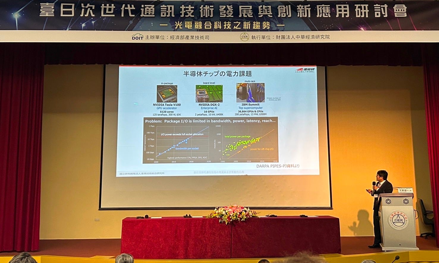
In today's era of rapid technological advancement, the wave of Artificial Intelligence (AI) is sweeping the globe with unprecedented force, creating an almost insatiable demand for computing power. To meet this challenge, the semiconductor industry is undergoing a profound transformation. Dr. Vincent Lin, Director of Advanced Technology Development in Corporate R&D at ASE Group, in his presentation titled "Advanced Packaging Evolution: Chiplets and Silicon Photonics-CPO," deeply analyzed the core technologies and future prospects of this trend.

The presentation began by highlighting that the explosive growth in AI computing needs is the fundamental driving force behind semiconductor technology evolution. Subsequently, the outline clearly delineated the roadmap for this technological progression: first, the initial evolution of advanced packaging, represented by "Chiplets" technology; second, a further evolutionary stage focusing on "Photonics & Co-Packaged Optics (CPO)"; then, an exploration of "Silicon Photonics (SiPh) Packaging" trends and a necessary "Toolbox"; and finally, an address of the "CPO & supplier chain challenges." This series of topics systematically showcased how semiconductor packaging technology is responding to the challenges of the AI era.

Why is such complex technological innovation necessary? The answer can be partly understood by drawing an analogy to a familiar problem: traffic congestion on our roads. Just as physical roads can become overwhelmed, leading to gridlock and delays, the "digital roads" that carry vast amounts of data for complex AI systems can also become critical bottlenecks, hindering performance.
One slide in the presentation, "Challenges Facing Human Society-Traffic," vividly illustrated this physical world constraint. This chart revealed the severe problems of modern urban transportation: up to 50% of big city areas are occupied by roads and car parking, the average utilization of familiar cars is merely 5%, and urban residents spend an average of 50 minutes commuting daily. More alarmingly, according to statistics from the World Bank & WHO, 1.2 million people die in road traffic accidents globally each year, with another 15 million seriously injured. These figures underscore the immense waste of resources (land, time, and money) and severe societal costs associated with inefficient physical infrastructure.
Addressing these complex traffic issues, such as developing autonomous vehicles and smart traffic management systems, heavily relies on powerful AI computing capabilities. However, these AI systems are incredibly data-hungry, akin to needing a massive influx of vehicles (data packets) to reach their destinations (processing units) efficiently. If the data pathways – the "digital bandwidth" – are too narrow, much like congested city streets during peak hours, the entire AI system slows down. This "digital traffic jam" results in processing delays, reduced responsiveness, and an inability for the AI to perform optimally when making critical, real-time decisions. This, in turn, validates the urgent need not only for high-performance, low-power chips but also for advanced packaging technologies capable of providing the massive bandwidth required to keep these digital highways clear and data flowing freely.
For Paid Members, SemiVision will discuss topics on
Top Companies by Capitalization in the world - AI Migration , what’s next wave ?
New Generation 3C - AI Centric - GPT / AI / ML
Evolution 1 Discussion - AI chip design
Evolution 2 Discussion - Optical Interconnection
CPO & supply chain challenges
SemiVision’s Viewpoint on ASE’s Advanced Packaging Strategy