

From Rice Fields to AI Chips: How TSMC Is Turning Chiayi into Taiwan’s Next Advanced Packaging Hub
Original Article By SemiVision Research [Reading time: 11 mins]

From Rice Fields to AI Chips: How TSMC Is Turning Chiayi into Taiwan’s Next Advanced Packaging Hub
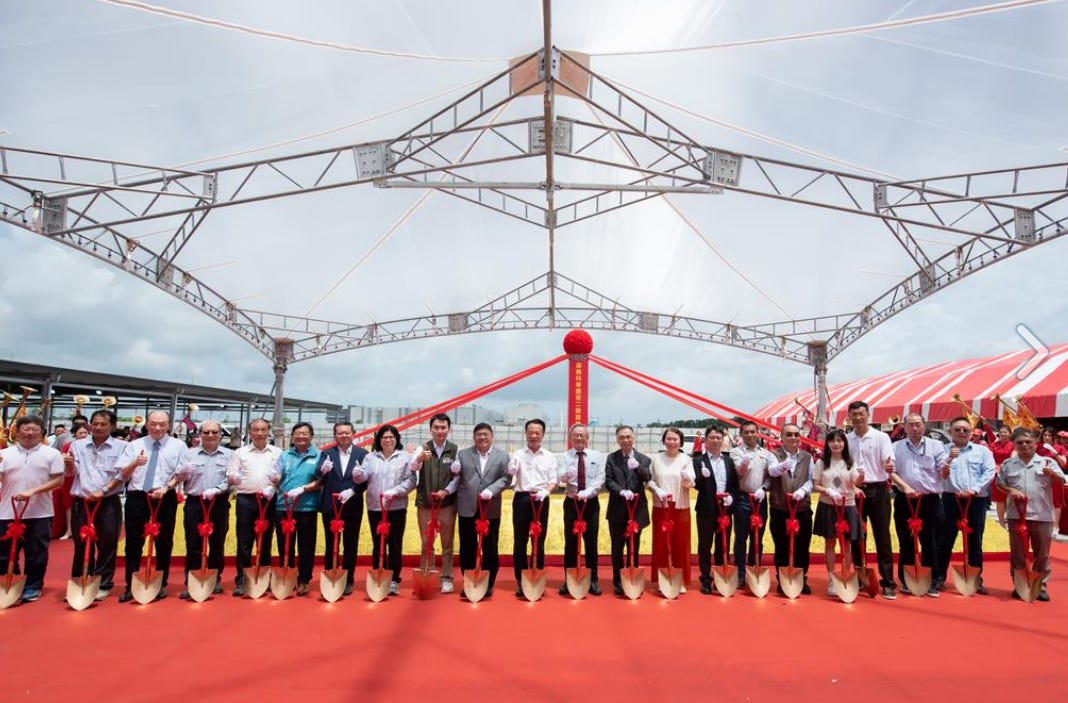
The groundbreaking of Chiayi Science Park Phase 2 may appear to be another 90-hectare industrial development project. However, viewed through the structural growth of AI chips, HBM, and advanced packaging, it represents a much larger transformation in Taiwan’s semiconductor industry.
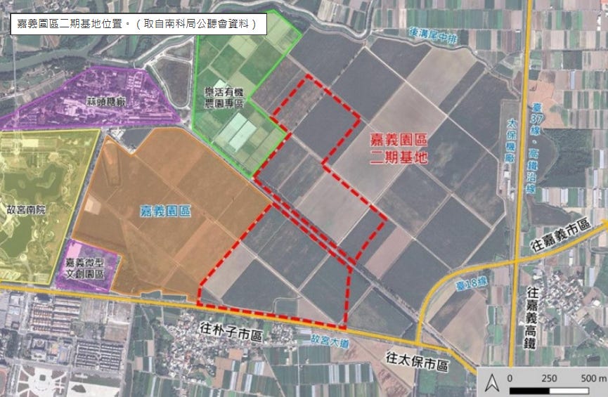
In the past, discussions about semiconductor clusters focused primarily on where a new wafer fab would be built, which process node it would use, and how many wafers it could produce each month.
In the AI era, however, the factors determining chip performance and delivery capacity have expanded far beyond front-end wafer fabrication.
Logic chips, HBM, silicon interposers, redistribution layers, package substrates, thermal-management solutions, testing systems, and dozens of specialized equipment and material categories must now be integrated within increasingly large and complex packages.
Advanced packaging is therefore no longer simply the “back end” of semiconductor manufacturing. It has become one of the core manufacturing technologies behind modern AI systems.
The development of Chiayi Science Park Phase 2 is a physical manifestation of this structural change—reshaping Taiwan’s industrial land, infrastructure, manufacturing capacity, and semiconductor supply-chain geography.
From an Agricultural County to an Advanced Packaging Hub
On July 12, 2026, the groundbreaking ceremony for Chiayi Science Park Phase 2 was officially held.
Located adjacent to Phase 1, the Phase 2 site covers nearly 90 hectares. The overall development is expected to be completed around 2031, with TSMC taking the lead in building an industrial cluster centered on advanced packaging.
More importantly, Chiayi Science Park is no longer merely a policy proposal or a project that exists only on a government planning document.
According to the Southern Taiwan Science Park Bureau and multiple media reports, TSMC’s advanced packaging operation in Chiayi Science Park Phase 1 began mass production in June 2026. Construction of facilities related to Phase 2 is proceeding in parallel, while public infrastructure—including wastewater treatment facilities, water-distribution reservoirs, and multifunctional buildings—is also being developed simultaneously.
In other words, Chiayi is rapidly moving beyond the land-preparation and investment-attraction stage. It is entering the phase in which actual manufacturing capacity and a surrounding supply-chain ecosystem begin to take shape.
This development speed is strategically important.
The competitiveness of a science park has never depended solely on inexpensive land. It depends on whether administrative approval, environmental reviews, electricity, water, roads, wastewater treatment, talent availability, and supplier services can all be delivered on schedule.
The greatest risk in semiconductor construction is often not the delay of a single building. The real danger is that the fab is completed while the external infrastructure or supporting supply chain remains unprepared.
Chiayi Science Park is currently pursuing a parallel-development model in which public infrastructure, corporate facility construction, and industrial recruitment are being advanced at the same time.
For TSMC, this can shorten the time required to bring new capacity online. For suppliers, it means the optimal time to establish a presence in Chiayi may arrive well before the entire park is formally completed.

How Should We Interpret the US$9.3 Billion Output Target?
There has been some confusion regarding the projected output and employment figures for Chiayi Science Park. This is mainly because some reports refer only to Phase 2, while others calculate the combined economic contribution of Phases 1 and 2.
According to development plans for Phase 2, the approximately 89.58-hectare site is expected to generate around US$6.5 billion in annual revenue once fully operational, while creating approximately 3,500 jobs.
In addition to advanced packaging, the park is expected to attract companies involved in heterogeneous integration, artificial intelligence, high-speed communications, cybersecurity, net-zero technologies, and quantum technology.
When Phases 1 and 2 are calculated together, official projections and related reports estimate that Chiayi Science Park could eventually generate more than US$9.3 billion in annual output and support more than 9,000 jobs.
However, SemiVision believes that the park’s strategic value cannot be evaluated solely through headline output and employment figures.
Advanced packaging is a capital-intensive and technology-intensive industry with an unusually dense supply chain.
The economic impact of a large packaging base extends beyond the direct output generated by TSMC. It also includes equipment maintenance, material replenishment, facility engineering, cleanroom construction, logistics, testing, substrates, thermal management, and a wide range of technical services.
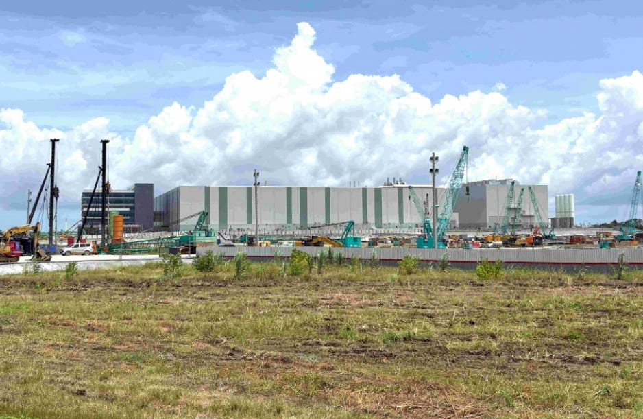
The true economic multiplier of Chiayi Science Park may therefore depend less on the number of companies formally registered inside the park and more on how many suppliers are required to establish warehouses, laboratories, field-application engineering teams, and rapid-response service capabilities across Chiayi and the broader Yunlin–Chiayi–Tainan region.
Why Does TSMC Still Need So Much Advanced Packaging Capacity?
The answer lies in the increasing size and integration complexity of AI chip packages.
Traditional semiconductor performance improvements were primarily achieved by shrinking transistors through more advanced process nodes. AI computing, however, requires such large logic areas, memory bandwidth, and I/O capacity that these requirements can no longer be addressed efficiently through a single monolithic die.
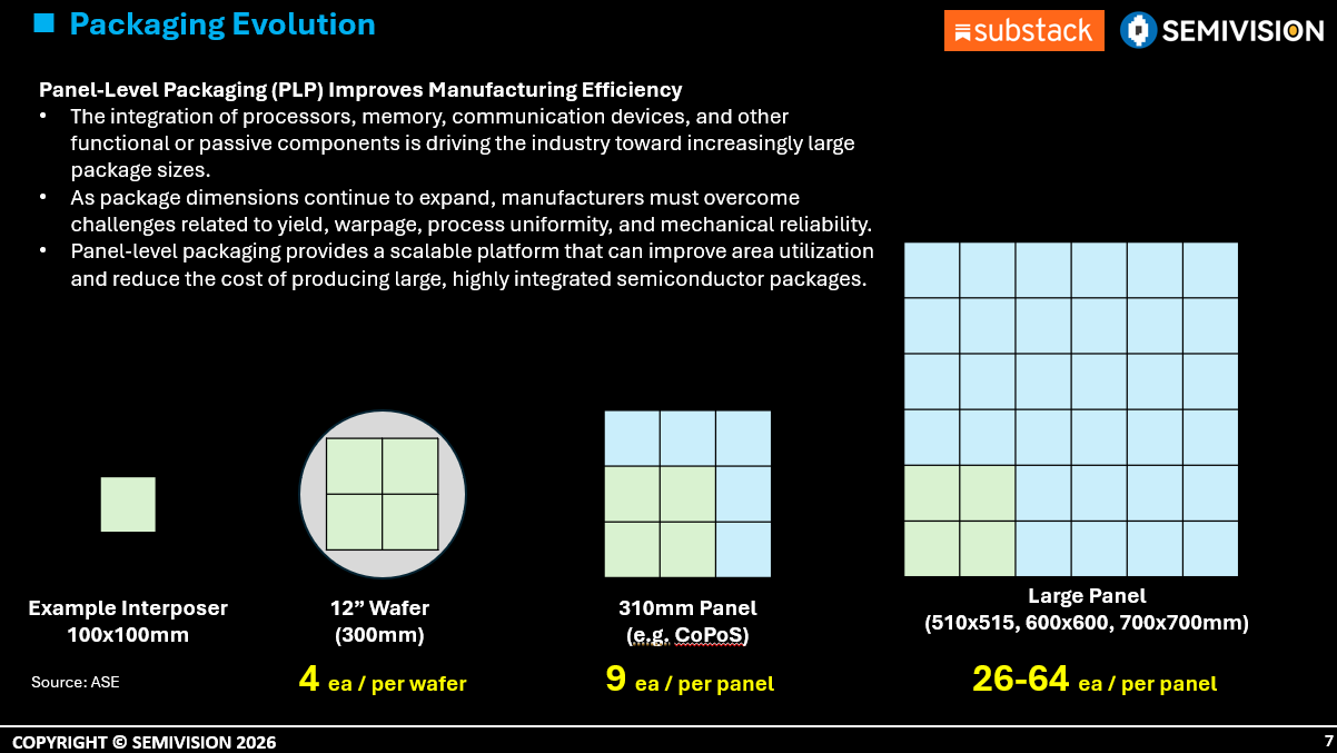
AI accelerators are therefore increasingly integrating multiple logic dies, HBM stacks, and specialized functional chips within the same package.
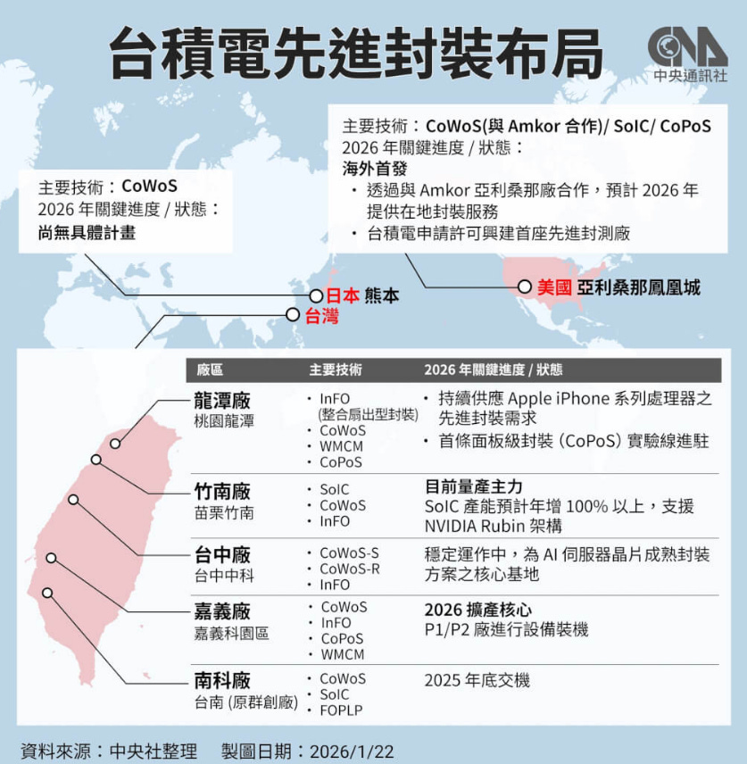
TSMC’s CoWoS platform uses technologies such as silicon interposers, redistribution-layer interposers, or localized silicon interconnect structures to integrate computing chips and HBM at extremely high interconnect densities.
At its 2026 Technology Symposium, TSMC indicated that it had entered production with CoWoS packages measuring approximately 5.5 times the standard reticle size.
The company is also planning to introduce a 14-reticle-size CoWoS architecture in 2028, potentially integrating approximately ten large computing dies and as many as twenty HBM stacks. Even larger architectures are expected to follow in 2029.
This development creates three direct consequences.
First, each package consumes more manufacturing area and equipment time.
Second, the number of packaging steps, material layers, and inspection points increases.
Third, a small manufacturing defect can result in the loss of multiple high-value logic dies and HBM stacks at the same time.
This means that even when AI chip shipment volumes do not increase at the same rate, the effective advanced packaging capacity, equipment footprint, and process-control capabilities required to support those shipments can still rise substantially.
The Chiayi expansion should therefore not be interpreted as merely replicating existing CoWoS production lines. It is also about preparing sufficient industrial space for the next generation of larger and more complex AI packages.

Chiayi Will Not Replace Hsinchu or Tainan—it Will Create a New Division of Manufacturing Roles
Taiwan’s semiconductor industry has historically been concentrated in Hsinchu, Taichung, and Tainan.
This concentration has created major advantages, including a dense supplier network, easier talent mobility, and faster technical support. However, as the industry expands, excessive concentration also creates pressure on land, water, electricity, transportation, housing, and engineering talent.
Chiayi occupies a strategically valuable position between the Tainan semiconductor cluster and central Taiwan’s supply-chain base.
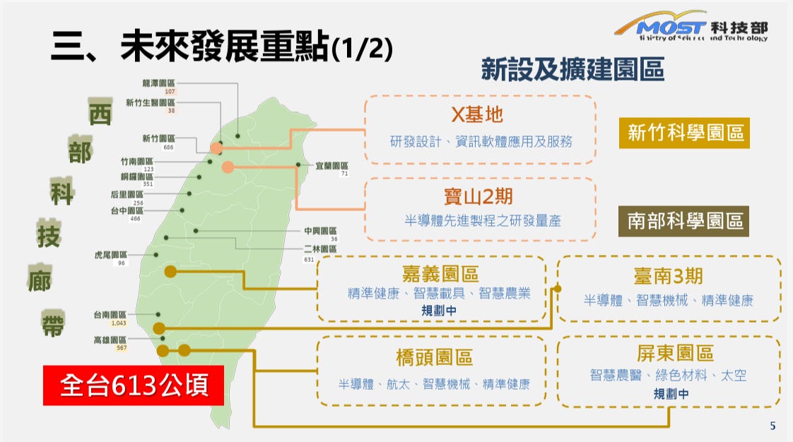
Through Chiayi Science Park Phases 1 and 2, together with the science and industrial parks in Tainan, Kaohsiung, and Pingtung, the government is seeking to build a southern technology corridor covering advanced process manufacturing, advanced packaging, AI servers, aerospace, drones, and downstream applications.
This southern corridor can then connect northward with the Central Taiwan Science Park and Hsinchu Science Park.
From TSMC’s perspective, this geographical configuration serves at least four functions.

First, it expands the amount of usable industrial land
Advanced packaging facilities do not necessarily require exactly the same fab architecture as leading-edge front-end wafer plants. Nevertheless, large cleanrooms, automated material-handling systems, testing operations, and facility infrastructure still require substantial space.
Second, it reduces the risk of excessive capacity concentration
Distributing advanced packaging capacity across locations such as Zhunan, Taichung, Tainan, and Chiayi can improve production flexibility and operational resilience.
Third, it brings packaging capacity closer to southern Taiwan’s advanced-node fabs
As advanced process capacity continues to expand in Tainan and Kaohsiung, a more closely connected southern manufacturing network between front-end wafer production and back-end advanced packaging can reduce logistics distances and improve engineering coordination.
Fourth, it preserves flexibility for long-term technology development
Future advanced packaging operations may need to support CoWoS, SoIC, wafer-level integration, silicon photonics, and increasingly complex testing processes.
The value of a large manufacturing site is that it can be reconfigured as technologies evolve rather than being locked into a single product generation.

The Beneficiaries Will Extend Far Beyond Traditional OSAT Companies
The greatest supply-chain impact of Chiayi Science Park Phase 2 will come from the additional demand it creates for equipment, materials, infrastructure, and engineering services.
On the equipment side, potential demand categories include:
Wafer and die bonding systems
Lithography and redistribution-layer equipment
Electroplating systems
Cleaning equipment
Grinding and thinning tools
Metrology and defect-inspection systems
Laser-cutting equipment
Temporary bonding and debonding systems
Molding and encapsulation equipment
Automated material-handling systems
Final testing equipment
On the materials side, demand may extend to:
Photoresists and dielectric materials
Electroplating chemicals
Underfill materials
Molding compounds
Temporary bonding adhesives
Cleaning chemicals
Advanced package substrates
Thermal-interface materials
High-purity process consumables
As package dimensions increase, controlling warpage, coefficient-of-thermal-expansion mismatches, surface flatness, particle contamination, and long-term material reliability becomes increasingly important.
Architectures such as CoWoS must simultaneously address high-density interconnections, signal integrity, power integrity, and thermomechanical stress between different materials. As a result, the technical barriers facing suppliers will also rise.
However, this does not mean that every company associated with the broad “advanced packaging” theme will benefit equally.
SemiVision believes that investors and industry participants should evaluate potential beneficiaries based on at least four conditions:
Has the supplier already passed qualification by TSMC or another major advanced packaging customer?
Does its product directly address a yield or capacity bottleneck in next-generation large-format packaging?
Can the company provide rapid technical support and spare-parts or material inventory in Chiayi or southern Taiwan?
Is its revenue growth coming from actual production shipments rather than sample deliveries, evaluation projects, or memoranda of understanding?
Chiayi’s expansion will create new demand, but those orders will not be distributed evenly across the supply chain.
Companies positioned closest to critical process steps, yield management, and high-frequency consumables are likely to have the highest degree of earnings visibility.

Chiayi’s Next Challenge: Moving from Rapid Construction to Stable Mass Production
Chiayi Science Park has already demonstrated considerable administrative and construction efficiency. The next stage, however, will be significantly more difficult.
The first challenge is talent
Advanced packaging requires process, equipment, materials, quality, testing, automation, and facility engineers.
Whether Chiayi can attract these professionals to live and work in the region over the long term will depend on more than compensation. Transportation, housing, education, and overall quality of life will also matter.
The establishment of an experimental high school and other public infrastructure is only the beginning. The region will eventually need a much more complete urban environment capable of supporting thousands of engineers and their families.
The second challenge is supply-chain localization
Equipment failures and material abnormalities cannot wait several hours—or until the following day—for technical support.
Whether key suppliers are willing to establish local service centers, laboratories, warehouses, and field-engineering teams in Chiayi will directly affect production stability.
The third challenge is water, electricity, and environmental management
Advanced packaging generally consumes less water and electricity than the most advanced front-end wafer manufacturing processes.
However, as cleanroom space, automated equipment, testing capacity, and overall production volume continue to expand, the combined burden on electricity, water, wastewater treatment, and environmental infrastructure will still be significant.
Whether public infrastructure can be completed in coordination with corporate facilities will be critical to the park’s ability to ramp production smoothly.

The final challenge is manufacturing yield
Large AI packages integrate multiple high-value logic chips and HBM stacks. A packaging defect can therefore create a much greater financial loss than it would in a conventional semiconductor product.
What will ultimately determine whether Chiayi becomes a global advanced packaging hub is not the number of groundbreaking ceremonies or factory buildings.
The decisive factor will be whether the region can establish a high-yield manufacturing system that is stable, scalable, and repeatable across multiple generations of AI products.
SemiVision View: Chiayi Marks the Beginning of a New Industrial Cluster Competition
Chiayi Science Park Phase 2 should not be interpreted simply as another production site added to TSMC’s manufacturing network.
It reflects a broader transformation in which AI chip competition is evolving beyond individual GPUs or process nodes into full-system competition involving memory, advanced packaging, equipment, materials, power, thermal management, data centers, and physical infrastructure.
As CoWoS evolves from integrating a limited number of chips and HBM stacks toward architectures containing ten computing dies, twenty HBM stacks, and eventually wafer-scale systems, the industry will need more than a single new production line.
It will require an entire ecosystem in which equipment, materials, talent, logistics, electricity, water, thermal management, and testing capacity can scale together.
Hsinchu established the foundation of Taiwan’s IC design and semiconductor manufacturing industries.
Tainan and Kaohsiung are absorbing the next wave of advanced process expansion.
Chiayi is now adding one of the most important missing pieces in the AI era: large-scale advanced packaging capacity.
Chiayi is unlikely to replace any existing science park.
A more accurate interpretation is that it will become a critical strategic node in Taiwan’s transition from a wafer-manufacturing advantage to a broader AI system-integration advantage.
The most important question is therefore not simply whether Chiayi Science Park Phase 2 can be completed by 2031.
The real question is how many equipment manufacturers, material suppliers, and technical service providers will begin incorporating Chiayi into their global AI supply-chain strategies over the next five years.
Taiwan’s rice fields form one of the island’s most distinctive rural landscapes. Stretching across fertile plains, they change color with the seasons—from mirrored paddies after planting to vivid green fields in summer and golden waves before harvest. Rice cultivation has shaped local communities, food culture, irrigation systems, and village life for generations. Farmers combine traditional knowledge with modern machinery to improve efficiency while preserving the land. Beyond food production, these fields support biodiversity, store water, and create peaceful scenery that reflects Taiwan’s close relationship with nature. They remain an enduring symbol of agriculture, resilience, and everyday life across Taiwan.