How Immersion Lithography Revolutionized Semiconductor Technology
Introduction of Dry and Immersion Lithography
Lithography is a cutting-edge technique used to create extremely small patterns on semiconductor wafers, enabling the production of next-generation microchips. It uses extremely short wavelengths to improve resolution and patterning precision.
Here is two types of lithography: Dry and Immersion systems
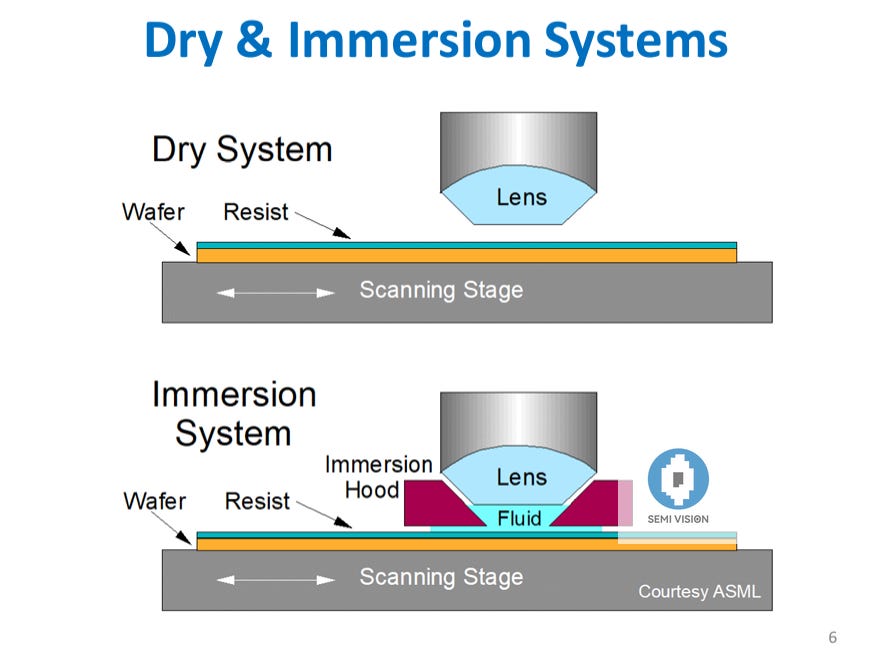
Dry Lithography:
In dry lithography, the process occurs in a vacuum without any liquid medium between the wafer and the lens.
This method is primarily used for earlier lithography systems and is simpler in terms of system design. However, the resolution is limited due to the lack of a refractive medium that can enhance the light's focusing ability.
It is well-suited for applications where moderate resolution is acceptable, and it requires fewer complexities in machine setup.
Immersion Lithography:
In immersion lithography, a liquid, typically water, is introduced between the lens and the wafer, enhancing the resolution by increasing the numerical aperture (NA) of the system.
The immersion technique allows more precise patterning at smaller scales, making it ideal for advanced chip manufacturing, especially in smaller nodes like 7nm and beyond.
Immersion lithography can achieve higher resolution than dry lithography, but it requires more complex system engineering and maintenance.
History of Immersion lithography
In the past, the industry used "dry" lithography technology. When a light beam passes through the photomask and lens and is projected onto the wafer, the medium between the lens and the wafer is air. Due to the significant difference in refractive indices between the lens (n=1.5) and air (n~1), the interface reflection is large, which reduces the resolution. To address this, Dr. Burn J. Lin immersed the lens and wafer in water, replacing air with water. Since the refractive index difference between the lens and water (n=1.44) is smaller, it effectively reduces the wavelength to 134 nanometers, thereby improving resolution. In 2004, Dr. Burn J. Lin, in collaboration with ASML, developed the first immersion lithography prototype.
Thanks to immersion lithography technology, TSMC not only leads the global semiconductor industry but also, after Dr. Burn J. Lin successfully persuaded equipment manufacturers like ASML and Nikon, immersion lithography officially entered the global market. This technology helped propel semiconductor advancements into the 7nm era within just over a decade. Meanwhile, ASML, which invested in both EUV and immersion lithography technologies, gradually became a dominant player in the semiconductor equipment industry. Since then, Dr. Burn J. Lin has been regarded as the "Father of Immersion Lithography.
Benefits of Immersion Lithography
No problem with CaF2 lens quality and quantity.
No resist absorption and etch resistance issues.
No N2 purging concern.
No hard pellicle issue.
Conclusion: lithography, both dry and immersion types, plays a critical role in modern semiconductor manufacturing. While dry lithography is simpler and less complex, immersion lithography is capable of achieving the highest resolution and is essential for next-generation chip production.