

Hybrid Bonding at Scale: BESI’s Vision and Industry Evolution in 3D Integration
Original Articles By SemiVision Research ( IEEE ECTC , IEEE IITC ,BESI , TSMC , Nvidia, AMD , Intel ,TEL , Suss ,EVGroup , K&S , ASMPT ,AMAT , SHIBAURA ,SET , NYCU ,ITRI)


As AI and high-performance computing (HPC) continue to advance rapidly, chip architectures are shifting toward 3D stacking, chiplet disaggregation, and heterogeneous integration. The realization of these technologies heavily depends on continuous breakthroughs and scalable mass production of bonding technologies. In this field, one company has long held a critical position—BE Semiconductor Industries N.V. (Besi), based in the Netherlands.
Besi: A Key Driver of the Transition from Planar to 3D Advanced Packaging
Founded in 1995 and headquartered in Duiven, the Netherlands, Besi operates manufacturing, R&D, and service facilities across Malaysia, China, Singapore, and the U.S. The company specializes in designing and manufacturing high-precision assembly equipment for the back-end semiconductor process, particularly targeting advanced logic chips, memory, sensors, and photonic devices.
Besi’s product portfolio spans from traditional 2D packaging to cutting-edge 2.5D and 3D packaging technologies, excelling in the following four core areas:
Besi’s Strategic Role in Advanced Packaging

Market Leadership
Besi holds a 42% market share in die-attach equipment, maintaining its global leadership for years. Its product offerings span epoxy, soft-solder, flip-chip, stacked die, and multi-module applications.
High Throughput and Precision Integration
Besi’s flagship Datacon and Esec platforms deliver ±4 μm @3σ precision, enabling high-speed, high-yield manufacturing with ultra-fine chip spacing—perfectly suited for performance-critical applications.
AI and Data Center Demand as Growth Catalysts
With the rise of AI, 5G, HPC, and chiplet-based modules, Besi’s advanced packaging solutions have become a critical enabler. In Q1 2025, Besi’s order intake increased by 8.2% to €131.9 million, largely driven by hybrid bonding orders.
Hybrid Bonding: Besi’s Core Technological Contribution

Hybrid bonding is at the heart of Besi’s technology roadmap. As a key enabler of vertical chip stacking and high-density interconnects, it delivers lower latency, reduced energy consumption, and enhanced bandwidth/system performance.
Breakthrough Capabilities
<10 nm Alignment Precision: Besi’s tools enable atomic-level copper-to-oxide and oxide-to-oxide bonding, essential for 3D integration.
Thermo-Compression Integration: Platforms like 8800 CHAMEO ultra plus AC combine cleanroom-grade bonding and optical alignment to ensure high yield and tight pitch stacking.
Industry Collaboration and Market Penetration
In 2024, Besi received orders for hybrid bonding systems with 100 nm alignment capabilities, indicating readiness for next-generation nodes.
Strategic partnership with Applied Materials (AMAT) since 2020, deepening in 2025 as AMAT became Besi’s largest shareholder (9%), enabling tight integration from deposition to final assembly.


Financial Outlook and Strategic Significance
At its 2025 Investor Day, Besi elevated hybrid bonding to a core business pillar, raising long-term revenue targets to €1.5–1.9 billion with 40–55% operating margins.
Financial Times reported hybrid bonding revenues at €36M in 2023, projected to surge to €476M by 2026, potentially accounting for one-third of Besi’s total business.
Technology Leadership and Strategic Positioning
Besi leads the hybrid bonding segment with its exceptional precision (<10 nm), high-yield control, and ultra-fine interconnect density, positioning itself at the forefront of AI, HBM, and 3D-IC packaging innovations.
Together with Applied Materials and ASML, Besi is part of a vertically integrated supply chain pushing hybrid bonding into high-volume production.
Growth Trajectory
With increasing demand from AI infrastructure and data centers, Besi is successfully transitioning hybrid bonding from a niche technology into a major revenue engine, showing strong long-term growth potential.

Why Should We Pay Attention to Hybrid Bonding Technology?
What Are the Challenges, and Where Is Advanced Packaging for AI Chips Heading?

These are all critical questions worth exploring. TSMC, for instance, is actively advancing its SoIC technology, which is fundamentally a 3D stacking architecture. This reflects the industry’s broader shift toward higher levels of integration and performance.
Hybrid Bonding: A Core Enabler for the New Era of 3D Chip Design

Hybrid bonding is regarded as one of the most transformative innovations in semiconductor manufacturing since extreme ultraviolet (EUV) lithography. Not only does it significantly improve the precision and performance of chip stacking, but it also redefines how chip designers approach 3D architectures and system integration.
Whereas EUV focuses on scaling within a single die, hybrid bonding opens up a new dimension—literally—enabling vertical stacking of multiple dies. It has become an essential technology for the advancement of advanced packaging and high-performance computing.
In the semiconductor industry, bonding technology plays a pivotal role in enabling heterogeneous integration and high-density 3D stacking architectures. As 3D ICs, chiplet-based designs, and advanced packaging technologies continue to gain traction, traditional bump-based or solder reflow methods are increasingly insufficient to meet the demands of finer pitches and high-speed data transmission. In contrast, hybrid bonding, which involves wafer-to-wafer (W-W) or die-to-wafer / die-to-die (D-W / D-D) alignment and interconnect, has emerged as the mainstream solution driving high-performance computing (HPC), AI chips, and memory stacking.
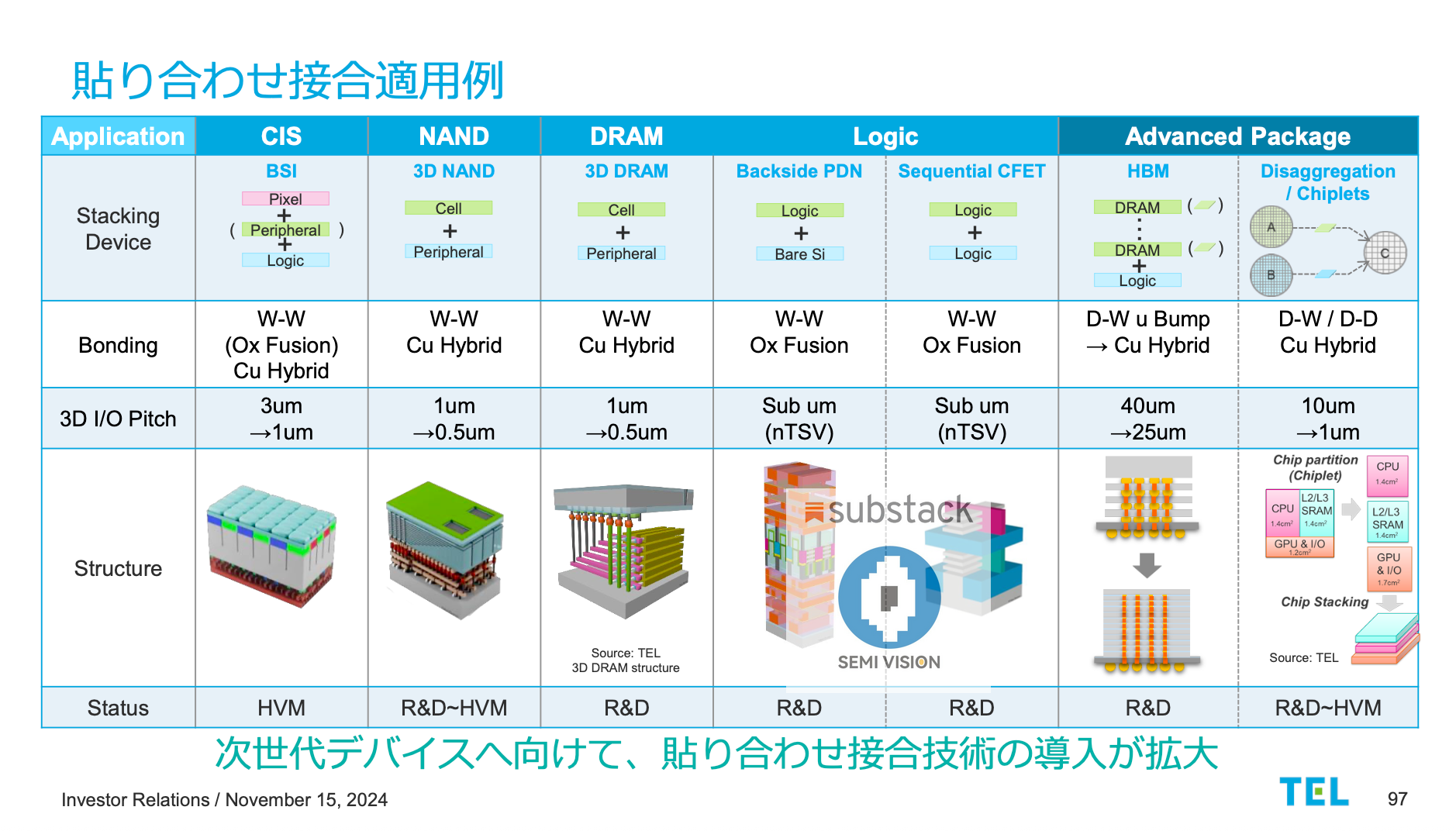
According to Tokyo Electron (TEL), bonding technologies are now widely applied across various device types, including CIS image sensors, 3D NAND, DRAM, logic ICs, backside power delivery (PDN), sequential CFETs, and advanced packaging scenarios such as HBM and disaggregated chiplets. Each application demands different levels of bonding precision and interconnect pitch—from 40 µm for early-generation memory stacks down to sub-micron and even <1 µm interconnects for next-generation chiplet architectures.

In advanced packaging, hybrid bonding not only increases I/O density and improves signal integrity, but also enables low-power, high-bandwidth heterogeneous integration. It is the foundational technology behind major 3D packaging platforms such as TSMC’s SoIC, Samsung’s X-Cube, and Intel’s Foveros. Looking ahead, as logic and memory stacking become more tightly coupled and bandwidth requirements continue to rise, bonding technology will only grow in importance—serving as a key enabler of innovation at both the chip and system levels.
1. Technical Principles and Architectural Characteristics
Hybrid bonding is a semiconductor stacking technology characterized by its bump-less interconnect structure. Unlike traditional solder-based packaging, hybrid bonding achieves both electrical and mechanical interconnection through direct copper-to-copper (Cu-Cu) contact. The top and bottom chips are bonded tightly, with only ultra-fine patterned copper pads encapsulated in dielectric material between them. These Cu pads typically have pitches below 10 µm and connect to internal chip metal layers through through-silicon vias (TSVs), forming complete signal and power paths.
The term “hybrid” refers to the combination of dielectric-to-dielectric molecular bonding and metal-to-metal copper bonding, both formed without adhesives. This results in a more stable, low-loss interface with excellent electrical and thermal properties.
2. Technical Advantages and System-Level Benefits
Hybrid bonding provides numerous technological and system-level advantages that are fundamentally reshaping chip design and system architecture:
Ultra-high interconnect density: Enables vertical interconnects at sub-10 µm, even down to hundreds of nanometers, far exceeding the density of traditional bump-based approaches.
Low resistance and reduced power: Eliminating solder bumps significantly reduces interconnect resistance, enhancing energy efficiency and thermal performance—crucial for high-speed data paths.
Low latency and short interconnects: Dramatically shortens signal paths to near on-chip distances, improving performance, particularly in AI, near-memory computing, and 3D cache architectures.
Architectural innovation: The high-density interconnect allows designers to modularize and heterogeneously integrate chip functions, overcoming single-chip area and yield limitations.
3. Manufacturing Challenges and Key Process Controls
Despite its transformative potential, hybrid bonding brings stringent process requirements. Critical factors include:
Surface flatness: Bonding interfaces are extremely sensitive to microscale roughness. Dielectric surfaces require <0.5 nm roughness, and Cu pads <1 nm. This necessitates chemical mechanical planarization (CMP) as a key step.
Cleanliness and particle control: Even a 1 µm particle can cause bonding failure across millimeter-scale regions. Hybrid bonding requires ISO Class 3 or better cleanroom environments, shifting it closer to front-end wafer fabs in cleanliness demands.
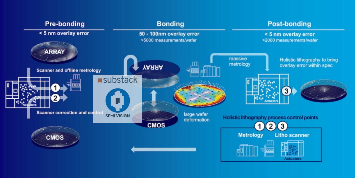
Alignment precision: Wafer-to-wafer (W2W) bonding systems must achieve sub-50 nm alignment accuracy, integrating high-resolution optics and precise mechanical positioning. Bonding pressure and dwell time must also be tightly controlled to enable initial van der Waals bonding and subsequent Cu-Cu bonding.
4. Process Overview
Hybrid bonding is implemented in W2W (wafer-to-wafer) or D2W (die-to-wafer) formats, following these general steps:
TSV formation: Establish signal and power paths in the base wafer through through-silicon vias.
Bonding layer fabrication: Deposit dielectric layers (e.g., SiO₂ or SiCN) and pattern Cu pads on wafer tops.
CMP planarization: Polish both bonding surfaces to meet nanometer-level flatness requirements.
Surface activation and cleaning: Treat with plasma (e.g., nitrogen) to activate surfaces, followed by DI water rinsing.
Alignment and pre-bonding: Align wafers using advanced positioning systems and apply low-pressure bonding to initiate dielectric adhesion.
Thermal annealing: Apply controlled thermal processing to form Cu-Cu metal bonds, finalizing the hybrid interface.
5. W2W vs. D2W Process Selection
W2W: Ideal for high-yield, small-area die; offers alignment and throughput advantages. Common in image sensors and 3D NAND.
D2W: Suitable for large or complex chips using known good die (KGD) after wafer sort. Technically challenging but enables modular, heterogeneous integration. AMD’s 3D V-Cache (SoIC) is a prominent example using D2W hybrid bonding.
6. Industry Applications and Leading Players

Hybrid bonding is currently deployed in CMOS image sensors, 3D NAND, and emerging high-end logic chips. AMD was the first to implement D2W hybrid bonding in commercial products. Leading equipment suppliers include:
BESI (Netherlands)
EVG (Austria)
Applied Materials (USA)
TEL – Tokyo Electron (Japan)
ASMPT (Singapore/HK)
SET (France)
SUSS MicroTec (Germany)
Shibaura Mechatronics (Japan)
These companies are aggressively developing hybrid bonding tools and ecosystems to support growing demand.
7. Process Positioning and Future Outlook
Hybrid bonding is increasingly regarded as a front-end-like process, demanding wafer fab-level precision and cleanliness. This raises barriers for traditional OSATs to enter without significant investment in cleanroom and tool upgrades. As AI, HPC, memory, and logic integration requirements grow, hybrid bonding is poised to become the standard 3D packaging interface—reshaping not just chip stacking but the entire system design and semiconductor manufacturing landscape.
The Future of Advanced Packaging: Decoding Besi’s Strategy in the AI Chip Stacking Era
As artificial intelligence and high-performance computing (HPC) drive semiconductor systems toward unprecedented levels of complexity and scale, back-end processes—once regarded as auxiliary—are now emerging as a critical frontier for innovation. At this pivotal moment, BE Semiconductor Industries N.V. (Besi), a leading packaging equipment provider based in the Netherlands, is positioning itself as a foundational enabler of the next generation of semiconductor manufacturing.
With deep investments in hybrid bonding, thermo-compression bonding (TCB), heterogeneous integration, co-packaged optics (CPO), and mobile chip stacking, Besi is not only delivering advanced tools but also shaping the strategic direction of the packaging ecosystem.
This article explores how Besi is evolving from a tooling provider into a central architect of the AI and chiplet-based packaging revolution. Drawing from insights in its investor presentations, we uncover not only the technical pillars but also Besi’s supply chain role, platform positioning, and competitive boundaries.
This article will cover the following key themes:
The evolution of AI chiplet package solutions: from 3D stacking and hybrid bonding to photonic integration and SoIC.
Performance advantages of hybrid bonding over traditional micro-bump: bandwidth density, power efficiency, and cost-effectiveness.
Industrial adoption of hybrid bonding by major players like Intel and Broadcom, including Foveros Direct and 3.5D XPU applications.
Technical analysis of CPO (Co-Packaged Optics) and hybrid bonding convergence: case studies of TSMC COUPE and Broadcom/NVIDIA implementation.
Bonding process evolution from HBM3 to HBM5 and how Besi’s tools align with this transition.
Frontier technologies in mobile and smartphone chip stacking: from InFO-PoP to SoIC-X/P platforms.
Besi’s strategic roadmap and its growth potential in the AI-driven end market.
This content will not only help you understand how Besi is positioning itself in the rapidly evolving landscape of advanced chip packaging but also serve as a gateway to mastering the hybrid bonding ecosystem. If you’re curious about the commercial roadmaps, supply chain transitions, and long-term competitive outlook of AI chip packaging, HBM, CPO, or SoIC, this article is your essential starting point.
For Paid Members, SemiVision will discuss topics on
Hybrid Bonding Supply Chain: A Global Overview
Advanced Packaging in the AI Era: BESI’s Strategic Bet on Hybrid Bonding
Hybrid Bonding at an Inflection Point
BESI at the Core of AI Packaging Transformation
Advanced Packaging in the AI Era: Global Capital Surge and BESI’s Central Role in the Supply Chain Transformation
TSMC Lead the Expansion of 2.5D/3D Packaging Capacity
Korea and the U.S. Target HBM and CPO Opportunities
Taiwan and China Fully Engaged; Europe Accelerating to Catch Up
Market Outlook: Advanced Packaging Becomes a Global Investment Focus
Rapid Growth in 2.5D/3D Packaging: BESI Accelerates High-Precision AI Assembly Solutions
Market Drivers: AI Workloads and Heterogeneous Integration
BESI’s Product Advantages: High Precision, High Contribution, High Growth
BESI Positions Itself at the Heart of AI Hardware Transformation
BESI Targets the Two Fastest-Growing Advanced Packaging Segments: Hybrid Bonding and Fluxless TCB
Fluxless Thermo-Compression Bonding: Emerging Use Cases with Strong Upside
BESI Expands Its Leadership in Die Attach and Advanced Die Placement for AI and Heterogeneous Integration
BESI’s Strategic Core: Centering on Advanced Packaging to Strengthen Its Leadership in Technology and Capital Allocation
BESI Accelerates R&D Investments to Power the Next Generation of Advanced Packaging Systems
Incidentally, a significant number of papers at recent IEEE ECTC and IEEE IITC conferences have focused on Hybrid Bonding technologies. Professor Chen from NYCU in Taiwan has published research utilizing Cu/Polymer Hybrid Bonding, while ITRI presented a novel Polymer-Based Hybrid Bonding technique through RDL interfacing at ECTC. Notably, Professor Chen has contributed numerous publications on 3DIC packaging in IEEE journals. In the future, SemiVision will be providing in-depth analysis on such innovative academic work.
BESI, in close collaboration with Applied Materials (AMAT), has also been actively engaged in Hybrid Bonding research. At IEEE IITC, BESI and AMAT co-authored a paper specifically focused on Die-to-Wafer (D2W) Hybrid Bonding, highlighting the depth of their technical partnership in advancing next-generation packaging technologies.


