

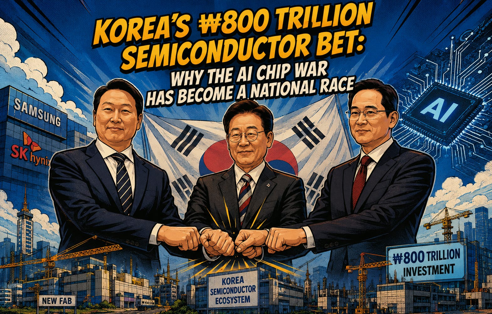
Korea’s ₩800 Trillion Semiconductor Bet: Why the AI Chip War Has Become a National Race
Original Article By SemiVision Research [Reading time: 14 mins]

Korea’s ₩800 Trillion Semiconductor Bet: Why the AI Chip War Has Become a National Race
The next phase of AI infrastructure will not be decided by one chip, one company, or one fab. It will be decided by national systems.
For the past two years, the semiconductor industry has been dominated by one powerful narrative: AI is creating shortages in HBM, advanced packaging, and the infrastructure required to build next-generation compute clusters. That narrative is still correct, but it is no longer sufficient.
South Korea’s June 29, 2026 announcement of an approximately ₩800 trillion semiconductor ecosystem plan marks a deeper shift. The AI chip race is no longer just Samsung versus SK hynix versus Micron, or TSMC versus Intel versus Samsung Foundry. It is becoming a competition between countries that can combine land, electricity, capital, talent, packaging capacity, data centers, materials, and policy into one integrated industrial machine. Reuters reported that Samsung Electronics and SK hynix will each build two new large-scale semiconductor fabs in South Korea’s southwest region as part of a national project to create a broader chip production ecosystem valued at around ₩800 trillion, or roughly US$518 billion.
This is why the announcement matters. It is not just another fab expansion plan. It is a signal that AI semiconductors are becoming national infrastructure.
From Company Competition to National System Competition
In the previous semiconductor cycle, the market usually asked a simple question: which company has the best technology roadmap? Investors compared process nodes, wafer capacity, yield, cost structure, and customer relationships. That framework still matters, but it is now incomplete.
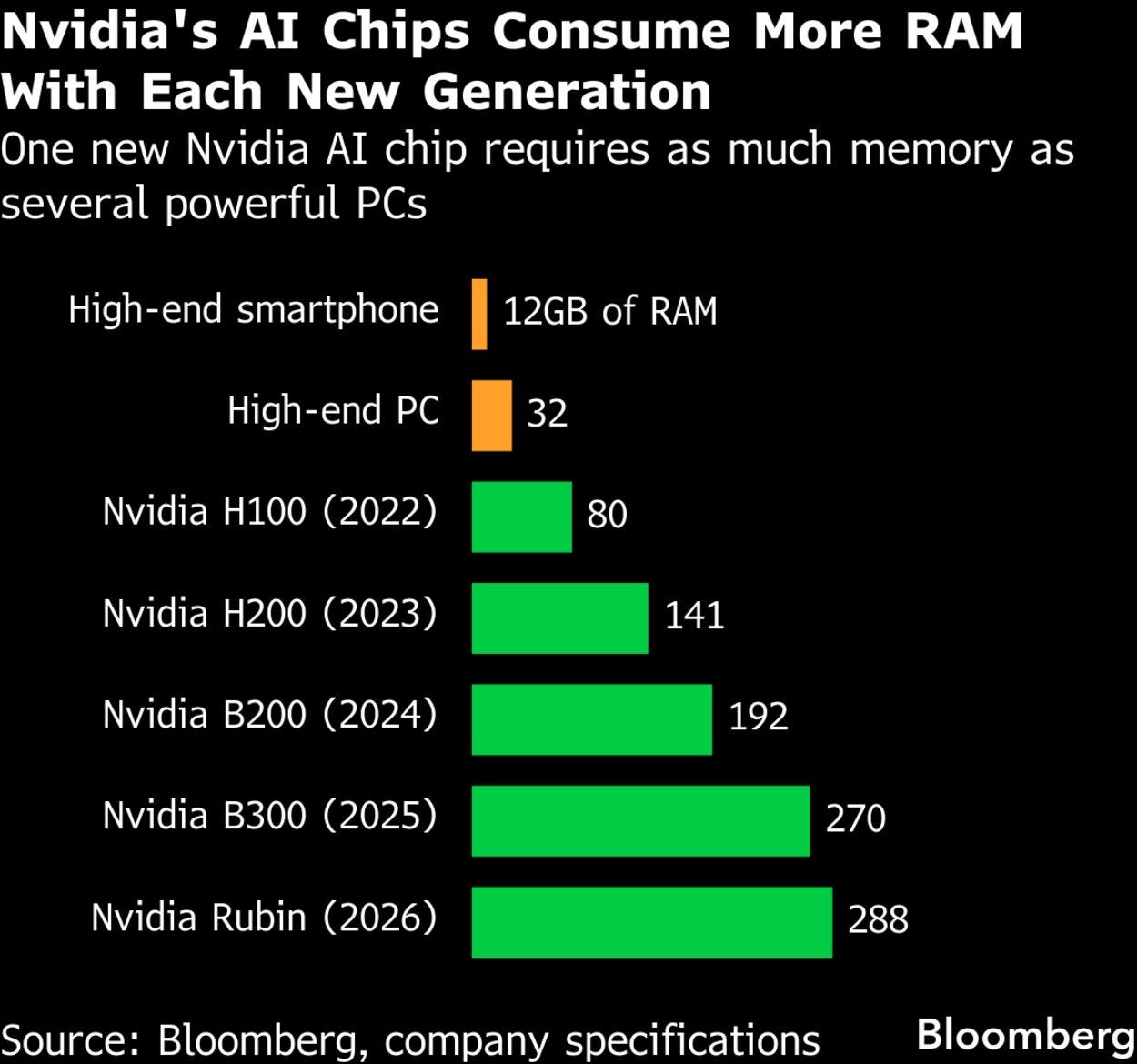
AI infrastructure requires a much broader supply chain. A GPU cannot ship without HBM. HBM cannot scale without advanced packaging. Advanced packaging cannot ramp without substrates, thermal materials, bonding equipment, inspection tools, and test capacity. Fabs cannot run without land, power, water, chemical supply, logistics, and skilled engineers. Data centers cannot expand without grid capacity and long-term energy planning.
This is the new semiconductor equation. The winner is not simply the company that designs the most powerful chip. The winner is the system that can reliably deliver complete AI infrastructure at scale.
South Korea appears to understand this. The country’s broader plan includes not only new semiconductor fabs, but also HBM capacity, a chip packaging cluster, AI data centers, and robotics initiatives. Samsung plans major domestic investments including semiconductor fabs in Gwangju and HBM fabs in Cheonan and Onyang, while SK hynix is planning a new chip production base in the southwest and continued expansion of its Yongin cluster.
This is not a normal memory-cycle expansion. This is industrial strategy.

Why AI Demand Is Different From the Smartphone and PC Era
The first reason South Korea’s plan matters is that AI demand is structurally different from the demand cycles that shaped memory in the smartphone and PC era.
In the old model, memory demand was mainly driven by consumer devices, enterprise servers, and replacement cycles. The industry was cyclical, but relatively understandable. When demand weakened, memory suppliers cut capex, reduced wafer starts, and worked through inventory. When demand recovered, pricing improved and investment resumed.
AI breaks that rhythm.
AI demand is more concentrated, more platform-based, and more long-term in nature. Large cloud companies and AI platform builders are not buying memory casually on a quarter-by-quarter basis. They are trying to secure multi-year supply for training clusters, inference platforms, custom ASICs, sovereign AI projects, and future data center buildouts.
Micron’s latest results show this shift clearly. The company reported record fiscal Q3 2026 revenue of US$41.46 billion, compared with US$23.86 billion in the prior quarter and US$9.30 billion a year earlier. More importantly, Micron said it had signed 16 strategic customer agreements that it expects will transform its business model. These agreements include US$22 billion in customer commitments, with structures such as take-or-pay clauses, cash deposits, and pricing floors.
This is the key insight: memory is no longer just a component. Memory is becoming supply security.
Memory Is Becoming a Strategic Asset Class
The memory industry has historically been treated as cyclical, volatile, and commodity-like. That view is becoming outdated at the high end of the market.
HBM, high-capacity DRAM, data center SSDs, and advanced memory subsystems are now becoming strategic assets. They determine whether AI accelerators can be shipped. They determine whether cloud customers can deploy clusters on time. They determine whether a platform can pass validation, hit bandwidth targets, and achieve acceptable power efficiency.
This is why long-term agreements matter. If customers are willing to sign multi-year contracts, provide deposits, accept pricing floors, or commit to minimum volumes, then the pricing mechanism of high-end memory is moving away from a purely spot-driven cycle. It is becoming closer to strategic allocation.
That changes the industry structure.
Large AI customers gain supply visibility. Memory suppliers gain revenue visibility. But smaller AI chip companies, second-tier cloud players, and weaker customers may face more difficulty securing stable access to premium memory. If HBM and high-end DRAM capacity are increasingly tied to long-term strategic customers, then the open market becomes thinner, less flexible, and more expensive.
This is one reason South Korea’s plan is so important. Samsung and SK hynix are not merely defending memory market share. They are trying to secure their position in the AI infrastructure stack before memory becomes even more deeply locked into platform-level supply agreements.
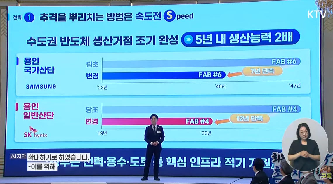
South Korea is accelerating its national semiconductor strategy under the banner of “speed.” The plan aims to complete the metropolitan semiconductor production hub earlier than scheduled and double production capacity within five years. Samsung’s Yongin National Industrial Complex Fab #6 timeline is being pulled forward by seven years, while SK hynix’s Yongin General Industrial Complex Fab #4 is targeted for a twelve-year acceleration. The message is clear: Korea wants to compress infrastructure, land, water, and power preparation into a faster national execution cycle, turning semiconductor manufacturing into a strategic platform for AI competitiveness, supply-chain resilience, and long-term technology leadership globally.
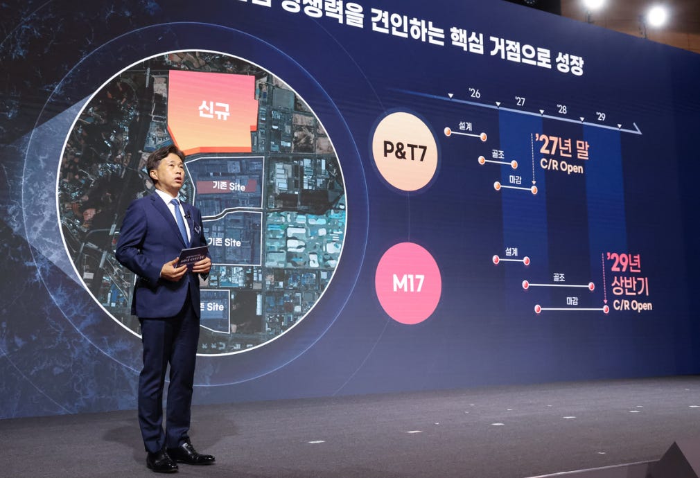
Under the plan, SK hynix will invest a total of 100 trillion won in Cheongju to build the M17 fab for NAND production and a Package & Test (P&T)7 facility to strengthen advanced packaging. Specifically, the company plans to invest 80 trillion won in M17, the new NAND fab, and 20 trillion won in P&T7 and other advanced packaging infrastructure. Construction of the new M17 fab is set to begin next year, with a target of starting operations in the first half of 2029. P&T7, which will handle advanced packaging, is scheduled for completion at the end of 2027.
At the SK Group level, the company is also pursuing the construction of a 1GW (gigawatt) AI data center in the Chungcheong region. The strategy is to create synergy by linking the chip production base with AI data center infrastructure. Source: sedaily.com
The Real Bottleneck Is Not Just Wafer Starts
The second reason this announcement matters is that the AI semiconductor bottleneck is no longer just wafer starts.
The industry often talks about capacity as if adding more fabs automatically solves the problem. But AI chips are not simple components moving through a linear supply chain. They are complex systems that require tight synchronization across multiple layers.
The bottleneck may appear in wafer fabrication. It may appear in HBM stacking. It may appear in advanced packaging. It may appear in substrate supply. It may appear in thermal materials. It may appear in testing. It may appear in power delivery. It may even appear in data center grid connections.
That is why the AI chip supply chain is becoming more fragile even as investment increases. A delay in one layer can delay the whole platform.
Samsung announced on May 29, 2026 that it had begun shipping 12-layer HBM4E samples to major customers, with speeds scalable up to 16Gbps and improved energy efficiency and thermal performance. SK hynix also said it had delivered 12-layer HBM4E samples to major customers, reaching up to 16Gbps per pin and using an advanced MR-MUF structure to reduce heat resistance.
But samples are not the finish line. In AI semiconductors, the real test is not who can announce the most advanced sample first. The real test is who can convert samples into qualified volume, stable yield, packaging throughput, customer certification, and predictable delivery.
That is where national-scale supply chain coordination becomes critical.
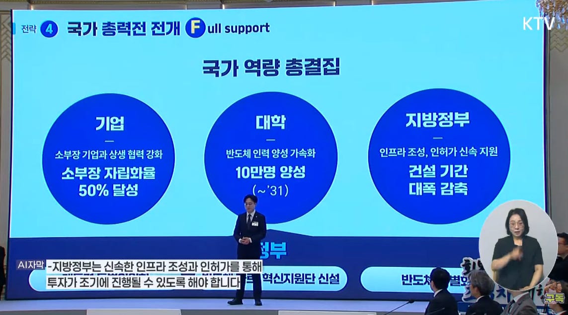
South Korea’s semiconductor strategy is shifting from company-led investment to full national mobilization. Under the “Full Support” pillar, the government is calling on enterprises, universities, and local governments to coordinate around one objective: faster semiconductor execution. Companies are expected to deepen cooperation with materials, parts, and equipment suppliers, with a target of reaching 50% supply-chain self-reliance. Universities will accelerate talent development, aiming to train 100,000 semiconductor professionals by 2031. Local governments will support infrastructure construction and fast-track permits to sharply reduce project timelines. The message is clear: Korea wants to turn semiconductor capacity into a national competitiveness platform.
Advanced Packaging Is Becoming the Command Center
For many years, packaging was treated as the back end of the semiconductor industry. That view no longer works.
In the AI era, advanced packaging is where memory bandwidth, interconnect density, thermal performance, power delivery, and system-level architecture meet. The package is no longer just a container for silicon. It is becoming the command center of AI performance.
This is why Korea’s packaging cluster deserves attention. The country is not only expanding memory fabs; it is also recognizing that advanced packaging is now central to AI infrastructure competitiveness. Reuters reported that South Korea’s broader plan includes an 81 trillion won packaging cluster in Chungcheong, alongside semiconductor and AI data center projects.
This is also consistent with global equipment trends. SEMI reported that global semiconductor equipment billings reached US$36.55 billion in Q1 2026, up 14% year over year, with record quarterly billings driven by AI-related investment in leading-edge logic, DRAM, and advanced packaging.
That combination is important. AI is not pulling only GPUs. It is pulling logic, memory, packaging, inspection, bonding, testing, substrates, power modules, cooling systems, and materials. The industry is becoming less like a chain and more like an orchestra. If one section misses the rhythm, the entire system falls behind.

Power, Water, and Land Are Now Semiconductor Weapons
The third reason South Korea’s plan matters is that infrastructure itself is becoming a competitive weapon.
A fab is not only a cleanroom. It is an energy system, a water system, a chemical system, a logistics system, and a human capital system. The same is true for AI data centers. The most advanced AI infrastructure cannot scale unless the surrounding region has enough power, land, permitting capacity, and technical labor.
Samsung and SK hynix plan to build the new semiconductor hub in South Korea’s southwest, with officials highlighting the region’s renewable energy potential and acknowledging challenges around power, water, and skilled workers. This detail matters more than many investors realize.
The semiconductor race is no longer only about process nodes. It is also about grid capacity.
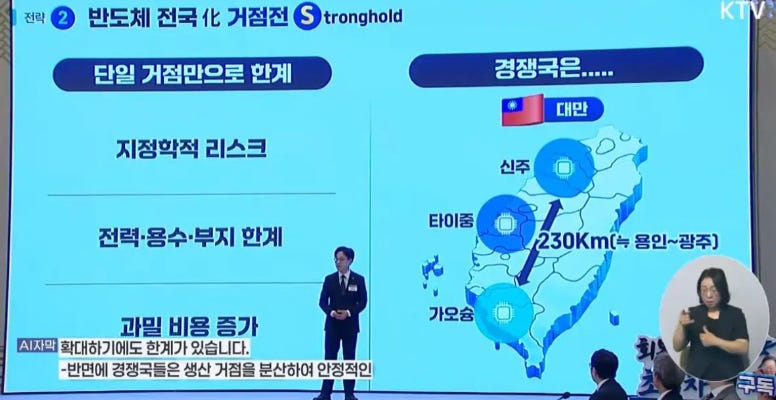
This is a direct warning to Taiwan, Japan, the United States, Europe, and emerging semiconductor investment regions in the Middle East. Fab announcements are easy. Grid connections are harder. Subsidies can be announced quickly. Talent clusters take years. Land can be allocated politically. But a complete semiconductor ecosystem requires decades of accumulated supplier density, engineering culture, and execution discipline.
AI is turning infrastructure into strategy.

Policy Is Reshaping the Supply Chain Map
The fourth layer is policy.
The United States is already redefining semiconductor supply through national security policy. In its January 14, 2026 proclamation on semiconductor imports, the White House directed the Secretary of Commerce to provide, by July 1, 2026, an update on the market for semiconductors used in U.S. data centers so the President could determine whether the tariff approach should be modified.
This means data center chips are no longer treated as ordinary commercial goods. They are increasingly viewed as strategic inputs for national power, AI leadership, and economic security.
South Korea’s timing is important. By announcing a national-scale semiconductor plan at this moment, Korea is sending a message to the United States, China, Taiwan, Japan, and global AI customers: Korea does not want to remain only a memory supplier. It wants to become a full AI semiconductor infrastructure hub.
That is a much larger ambition.
Memory leadership gives Korea leverage. HBM gives Korea strategic relevance. Advanced packaging gives Korea a path to move closer to system-level value. AI data centers give Korea a way to connect chips to domestic compute demand. Policy support gives the ecosystem durability.
This is how industrial power is built in the AI era.
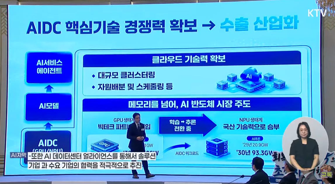
South Korea is positioning AIDC as a new export industry by securing core technologies across the AI data center stack. The strategy links AI service agents, AI models, and AI data centers into one national platform. Key priorities include large-scale clustering, cloud infrastructure capability, resource allocation, and scheduling technologies. Beyond memory leadership, Korea aims to expand into AI semiconductor markets by shifting workloads from GPU-centric ecosystems toward domestically developed NPU technologies. As AI training and inference demand rises, the government wants to build an AIDC ecosystem that connects solution providers, semiconductor companies, and end users, turning infrastructure into a scalable global business.
The Risk: Mega-Capex Does Not Solve Everything
Still, the ₩800 trillion plan is not risk-free.
The first risk is time. Large semiconductor ecosystems cannot be built overnight. AP noted that SK hynix’s major manufacturing cluster in Gyeonggi Province took nine years to establish. That means the new southwest hub may not solve the immediate HBM and advanced packaging shortages in 2026 or 2027. Near-term supply may remain tight even if long-term capex announcements look huge.
The second risk is over-capitalization. If AI demand remains strong through the end of the decade, Korea’s investment may look visionary. But if hyperscaler capex slows, if model efficiency improves faster than expected, if custom ASIC architectures reduce some memory intensity, or if customers diversify supply more aggressively, today’s heavy capital commitments may create return pressure later.
The third risk is execution complexity. Expanding beyond established semiconductor regions means suppliers must follow, engineers must relocate, utilities must scale, and local governments must execute. A fab is not valuable by itself. It becomes valuable only when the ecosystem around it is ready.
The fourth risk is geopolitical. If U.S. policy changes the rules around data center chips, advanced AI accelerators, or supply-chain localization, then Korea will need to balance its role as a global supplier with the strategic expectations of its major customers and allies.
In other words, Korea’s plan is bold. But bold plans still need flawless execution.

What Investors Should Watch Next
The market should not focus only on the headline number. The real signals will appear in the details.
First, investors should watch how Samsung and SK hynix allocate the new capacity. Is the focus mainly DRAM and HBM, or will the plan also support logic, foundry, and heterogeneous integration? The answer will show whether Korea is defending memory leadership or trying to move deeper into the AI system stack.
Second, watch the Chungcheong packaging cluster. If OSATs, substrate makers, materials suppliers, equipment vendors, and test companies begin committing capital together, the project becomes much more meaningful. Advanced packaging ecosystems cannot be built by memory makers alone.
Third, watch Micron. If Micron expands its strategic customer agreement model, the memory market may shift more permanently from spot-driven pricing toward contract-driven supply allocation. That would change how investors should value memory companies.
Fourth, watch U.S. policy after July 1, 2026. Any new conditions around data center semiconductors, tariffs, exemptions, or supply-chain localization could influence where future AI chip capacity is built.
Fifth, watch the response from Taiwan, Japan, and the United States. TSMC, Intel, Samsung Foundry, and OSAT players may need to clarify how they plan to scale 2nm, advanced packaging, local supply chains, and AI infrastructure support.
The most important question is not whether Korea’s number is big. The most important question is whether Korea can convert money into synchronized capacity.
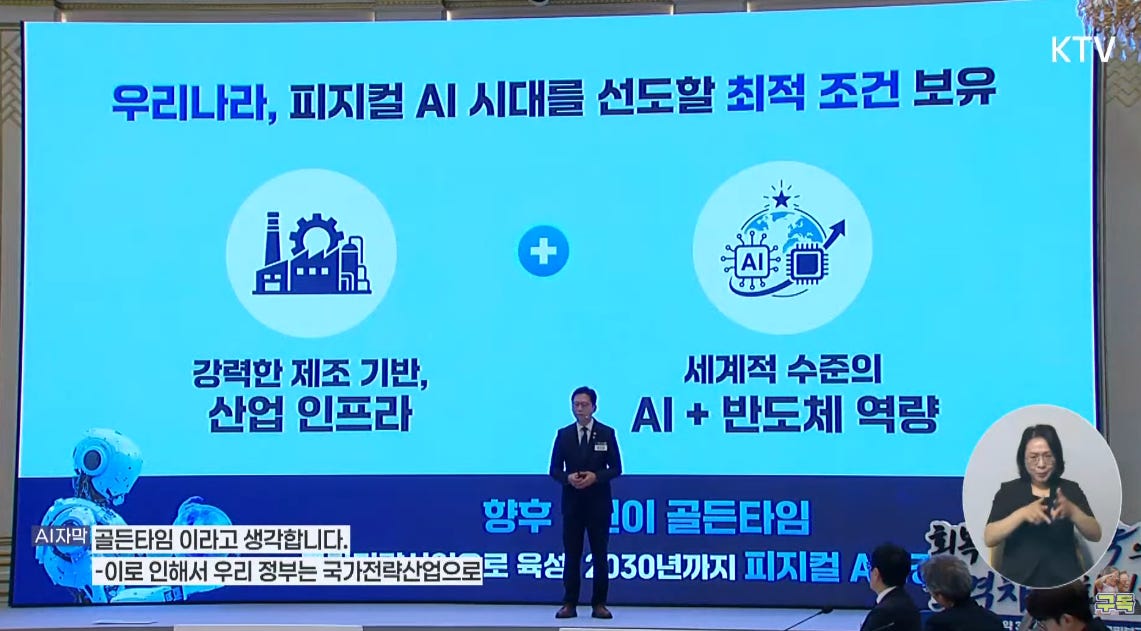
South Korea believes it has the optimal conditions to lead the Physical AI era: a powerful manufacturing base, deep industrial infrastructure, and world-class capabilities in AI and semiconductors. The message is that future AI competition will not be won by software models alone, but by the countries that can connect intelligence with factories, robots, chips, sensors, and real-world production systems. Korea sees the coming years as a golden window to scale Physical AI as a national strategic industry by 2030. With semiconductors at the core, the country aims to convert industrial strength into next-generation AI leadership for global competitiveness and resilience.

The SemiVision View: Capacity Alone Is Not Enough
The AI semiconductor cycle is often described as a supercycle. That may be true, but the phrase can be misleading. A supercycle does not mean every form of capacity will be rewarded equally.
The next winners will not simply be the companies that build the most fabs. The winners will be the companies and countries that can connect capacity with the right customers, the right packaging flow, the right power infrastructure, the right memory roadmap, and the right policy protection.
This is the deeper meaning of Korea’s ₩800 trillion bet.
The first stage of the AI boom was about GPUs. The second stage was about HBM. The third stage is about advanced packaging. The fourth stage may be about power. But the real story is that all four are now merging into one national infrastructure contest.
AI chips are no longer just products. They are becoming strategic systems.
And in this new era, the most important question is no longer: who can design the best chip?
The better question is: who can build the national system that keeps the AI infrastructure machine running