

More than Moore's law — Scaling with silicon photonics
Original Article by SemiVision Research (TSMC , Nvidia , Soitec)

More than Moore’s Law — Unlocking New Scaling Horizons with Silicon Photonics
The exponential growth of intelligent mobile devices, hyperscale computing, and the Internet of Things (IoT) is fueling an insatiable demand for instantaneous, ubiquitous access to massive datasets distributed across globally interconnected data centers. This relentless data explosion not only pressures system architects to deliver higher computational throughput but also exposes critical bottlenecks in traditional electronic interconnects, which struggle to scale energy efficiency, bandwidth density, and latency in next-generation systems.
While Moore’s Law historically delivered exponential scaling by shrinking transistor dimensions, the semiconductor industry now recognizes that transistor scaling alone is no longer sufficient to meet the demands of AI, cloud computing, and data-centric workloads. The “More-than-Moore” paradigm has emerged as a new scaling frontier, emphasizing heterogeneous integration, system-level co-design, and materials innovation as critical enablers of future performance and functionality.
In logic process scaling, CMOS scaling traditionally follows Moore’s Law. However, at several key nodes—for example, N2 adopting GAA (Gate-All-Around)—this trend is expected to continue toward nodes like A10. As for the future of CMOS, whether innovations such as CFET (Complementary FET) or new material breakthroughs will emerge remains an important area to watch.

Among these technologies, silicon photonics stands out as a transformative platform that extends scaling beyond electrical interconnects. By integrating optical waveguides, modulators, detectors, and multiplexers onto standard silicon wafers using CMOS-compatible manufacturing processes, silicon photonics enables low-latency, ultra-high-bandwidth, and energy-efficient optical communication directly on chip, across packages, and between systems. This advancement addresses the fundamental limitations of copper-based interconnects, such as high insertion loss, crosstalk, and excessive power consumption over long distances.
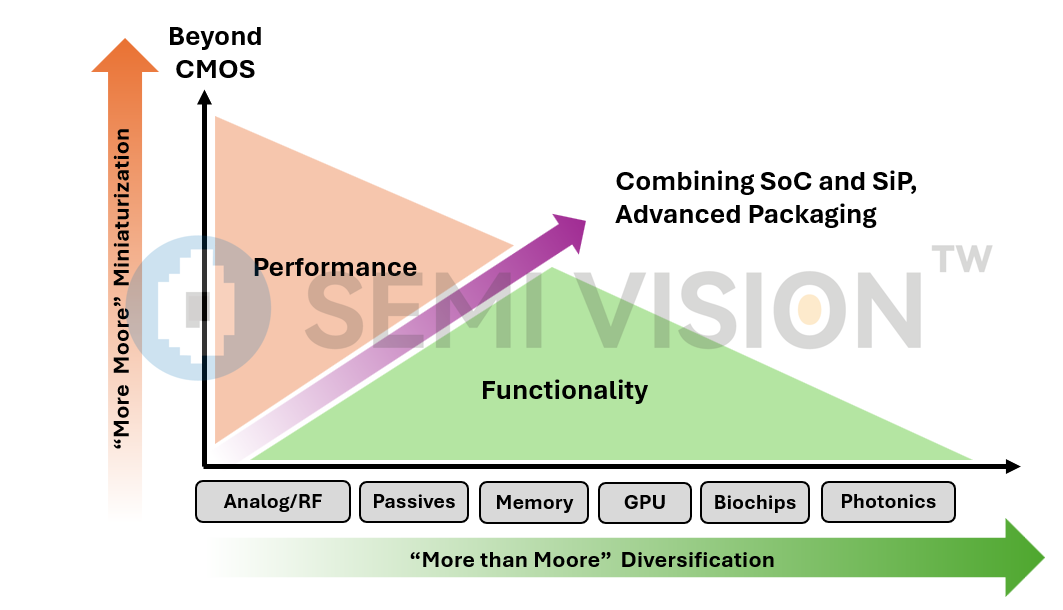
Moreover, silicon photonics opens new architectural possibilities by supporting chiplet-based designs, co-packaged optics (CPO), and disaggregated computing architectures, where optical links seamlessly interconnect memory, compute, and networking elements. These capabilities are increasingly critical in AI training clusters, high-performance computing (HPC) systems, and cloud-scale data centers, where data movement dominates system-level performance and power budgets.
Looking ahead, silicon photonics is evolving beyond passive waveguides to incorporate active materials innovations, such as electro-optic polymers, lithium niobate thin films (LNOI), III-V heterogeneous integration, and phase-change materials (PCM). These breakthroughs enable higher-speed modulators, lower-loss waveguides, and reconfigurable optical circuits, pushing the boundaries of integrated photonic performance.
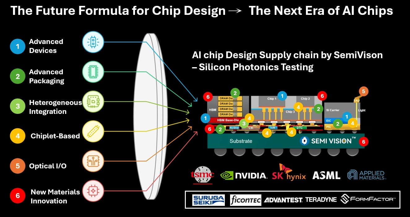
The Future Formula for Chip Design
Advanced Devices + Advanced Packaging + Heterogeneous Integration + Optical Interconnects + Chiplet-Based + Optical I/O + New Materials Innovation = The Next Era of AI Chips
Starting from this article, we will guide our readers through the theme of Scaling with Silicon Photonics and Material Innovation under More-than-Moore—diving deeper into how TSMC and the wider industry are pushing the boundaries of integration, performance, and manufacturability.
Device Scaling and the Photonic Substrate Era
TSMC’s Silicon Photonics Innovation Team Driving Industry Collaboration
Silicon Photonics: A Key Driver of the More-than-Moore Era
How Advanced Packaging and Silicon Photonics Work Together to Extend Moore’s Law
Heterogeneous Integration: Breaking the Limits of Monolithic Scaling
The Future Formula for Chip Design