

NVIDIA GTC – The Critical Step in CPO Technology: Optical Engine Testing – ficonTEC
Original Articles by SemiVision Research

NVIDIA GTC 2025 – The Overlooked Critical Step in CPO Technology: Optical Engine Testing
While NVIDIA GTC 2025 highlighted major advancements in Co-Packaged Optics (CPO) technology—such as co-integration with switch ASICs, improved energy efficiency, and system-level innovation—one critical step remains largely underdiscussed: Optical Engine Testing. This process is essential to ensure the functionality, performance, and reliability of the optical engine before it is permanently co-packaged with electronic components. Without a robust testing strategy, the entire CPO ecosystem faces risks in yield, thermal performance, and long-term system stability, making optical engine validation a crucial yet often overlooked enabler for scalable AI infrastructure deployment.
At GTC 2025, NVIDIA unveiled the world’s leading silicon photonics-based switch system, featuring advanced 200G SerDes technology. Compared with traditional pluggable optical modules, this innovative co-packaged silicon photonics technology offers significant advantages, including a 3.5× reduction in power consumption, lower latency, and substantially improved network reliability — all of which are critical for accelerating large-scale AI model development and inference.

What is Co-Packaged Silicon Photonics?
NVIDIA views this as a major evolution in hardware integration. By directly packaging silicon photonic transceivers with the switch IC, the company has achieved:
Lower Power Consumption: Compared to conventional pluggable optics, co-packaged optics (CPO) delivers a 3.5× power reduction. This is achieved by eliminating external DSPs and shrinking the signal path from inches to millimeters, dramatically improving energy efficiency. This denser and more sustainable AI infrastructure is designed to meet the growing demands of next-generation AI.
Component Reduction: Fewer discrete parts simplify manufacturing and reduce potential points of failure. Integrating optical components directly into the package eliminates the complexity associated with sourcing, assembling, and testing thousands of tiny discrete components found in traditional optical module systems.
Enhanced Performance: By integrating the optical engine at the package level, the connection between the switch ASIC and the photonic transceiver is optimized for performance, eliminating signal degradation and the need for external DSPs — which often introduce latency and consume significant power.
Simplified Data Center Operations: Reduced complexity in cabling and deployment leads to faster rollouts and easier maintenance.
Why It Matters
The benefits are evident. In a typical three-tier network architecture, one GPU requires six optical modules. Assuming each module consumes 30W and delivers 18.75 pJ/bit, a hyperscale AI cluster with 1 million GPUs would require 6 million optical modules — totaling 180MW in module power consumption.
With CPO, the power per port is reduced to 9W with an efficiency of 5.63 pJ/bit. The optical engine’s total power consumption drops to 54MW — a 30% reduction, aligning closely with figures previously published by Broadcom. Considering that each B200 GPU chip consumes approximately 1kW, the power savings from optical interconnects could power around 126,000 B200 chips.
Technical Highlights from GTC
Leaked details from the event reveal a highly integrated system involving EICs (electronic integrated circuits), PICs (photonic integrated circuits), 3D packaging, optical coupling, pluggable connectors, optical modules, external laser modules, laser chip packaging, interposers, and more.
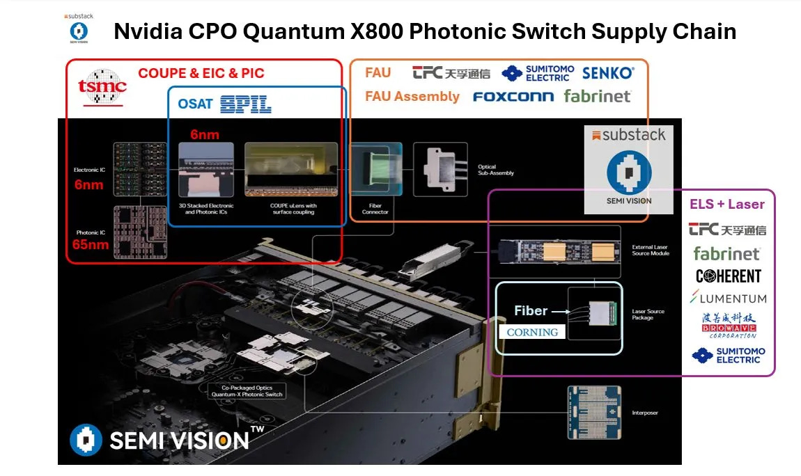
During his keynote, Jensen Huang emphasized that CPO is far more than photonic-electronic chip co-design; it encompasses advanced packaging, laser integration, optical packaging, structural engineering, and thermal solutions. NVIDIA leveraged its world-class supply chain to integrate technologies across domains, successfully bringing to mass production a CPO switch based on MRM (microring modulator) technology — thus ushering in the CPO era.
At NVIDIA GTC 2025, while the spotlight was placed on the company’s advancements in Co-Packaged Optics (CPO)—including its co-packaging architecture with switch ASICs, energy efficiency advantages, and system integration potential—one of the most critical and technically demanding aspects was noticeably absent from the discussion: Optical Engine Testing. The optical engine, as the heart of the CPO system, incorporates silicon photonic components (PIC), drivers, modulators, lasers (such as DFB or EML), and photodetectors. Its testing process is not limited to validating optical and electrical performance but must also ensure thermal stability, packaging compatibility, and manufacturing yield, all of which are foundational for ensuring reliability and scalability. Unlike pluggable optics, where full testing can be conducted before deployment, CPO integrates the optical engine directly alongside the ASIC or on the package substrate, making component replacement impossible after assembly. This imposes extremely stringent requirements for pre-packaging verification of all optical and electrical parameters. Key challenges include achieving sub-micron active optical alignment at the chiplet scale, executing wafer- or die-level optical yield scans and BER testing, and maintaining post-hybrid bonding stability and contact integrity. Currently, companies such as ficonTEC, FormFactor, EXFO, and Keysight are developing next-generation optoelectronic testing platforms to address these bottlenecks. In particular, ficonTEC has established a lead with its machine vision-assisted six-degree-of-freedom (6-DOF) active alignment, AI-driven performance optimization workflows, and automated optical probing technologies, enabling end-to-end validation from early optical engine packaging to pre-FAU array inspection. Notably, in the mass production phase of CPO, the optical engine testing process will not only determine the usability of individual modules but will also directly impact overall product yield, reliability, and delivery timelines. It is a critical enabler for widespread deployment and alignment with AI data center standards. While NVIDIA GTC 2025 emphasized the energy and integration advantages of CPO, the reality is that the viability of this technology depends heavily on yield management and manufacturing maturity across the supply chain. This makes high-precision optical testing capabilities from players like ficonTEC, as well as collaborative development with ODMs, an essential piece of the puzzle. Ultimately, whether the industry can build a robust “module-to-system” testing and validation chain will determine whether CPO becomes a scalable and commercially viable solution in the AI infrastructure of tomorrow.
For Paid Members, SemiVision will discuss the topics on
Nvidia Silicon Photonic Ecosystem
Role of ficonTEC in the Ecosystem
Ushering in a New Era of Silicon Photonics Mass Testing for the AI Age
ficonTEC Leads Silicon Photonics Testing Technology
Strategic Collaboration with JABIL
ficonTEC at ECTC 2023: Leading the Future of Adaptive Manufacturing in Photonic Integration
High-Volume Photonics Packaging: Opportunities and Challenges