

OFC50: TSMC’s Vision for Silicon Photonics — From Pure Foundry to System-Level Integration Platform
Original Article by SemiVision Reserch (TSMC , Nvidia)

TSMC’s Silicon Photonics Roadmap at OFC50
From Pure Foundry to Integrated Platform Enabler
At OFC 2025, TSMC unveiled for the first time a comprehensive and systematic overview of its strategy in the field of silicon photonics. The company is evolving from a pure-play wafer foundry into a full-spectrum technology enabler—encompassing design support, heterogeneous integration, standardized component platforms, and module-level photonic engines. This transformation reflects TSMC’s proactive response to the systemic challenges posed by AI and high-performance computing (HPC), particularly the growing demand for high-speed, low-latency, and energy-efficient interconnects.

The announcement highlights not only TSMC’s maturity in photonic device fabrication at the 65nm node and its integrated design automation capabilities, but also extends to its advanced packaging technologies such as SOIC-X for high-density 3D stacking and the forward-looking COUPE (Compact Universal Photonic Engine) platform. Together, these demonstrate TSMC’s strategic shift from a traditional foundry model toward becoming an integrated silicon photonics platform provider, tailored for next-generation applications in Co-Packaged Optics (CPO) and Optical I/O.
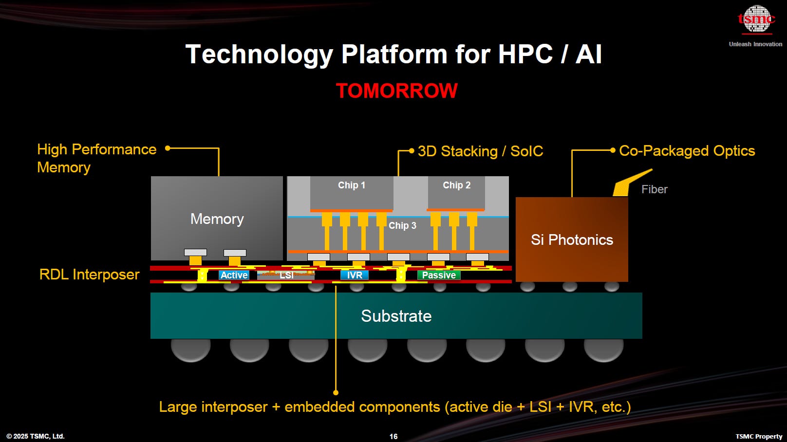
Against the backdrop of rapidly increasing data intensity and the shift toward chiplet-based architectures and optical interconnects in the AI era, TSMC’s platform transition carries three strategic implications:
From Process Technology to System Integration: TSMC is no longer just manufacturing photonic wafers, but now supports full-chain integration including co-design workflows, PDK openness, EDA interoperability, and optical test validation.
From Manufacturer to Ecosystem Enabler: Rather than competing with system companies, TSMC positions itself as a collaborative, non-competing partner to system-level players such as NVIDIA, Broadcom, and Marvell.
From Discrete Components to Structural Solutions: The silicon photonics platform is not merely an incremental technical upgrade—it’s a structural response to cross-generational demands in AI, HPC, LPO, CPO, and edge computing.
In essence, TSMC’s silicon photonics roadmap is more than a technical announcement—it is a value proposition for the future of data center and compute interconnect architecture. It signals TSMC’s ambition to become the wafer-scale infrastructure cornerstone of the photonic-electronic convergence era.
For Paid Members, SemiVision will discuss the following topics on :
Foundry + Platform — TSMC’s Value-Driven Transformation
Three Core Technology Pillars: Deep Integration from Device to Packaging
Silicon Photonics Process Platform and Modular PDK Infrastructure
SOIC-X: High-Density Interconnects for Electro-Photonic Integration
Value Proposition: Powering the Integrated Electro-Photonic Era for AI
From Foundry to Electro-Photonic Platform Architect