

Scaling Together: Netherlands x Taiwan Integrated Photonics Outlook from PIC Summit Europe 2025
Original Article By SemiVision Research ( PIC Summit, TSMC, ASE, Foxconn, Nvidia, PhotonDelta, ITRI ,HiSPA , TOSIA)


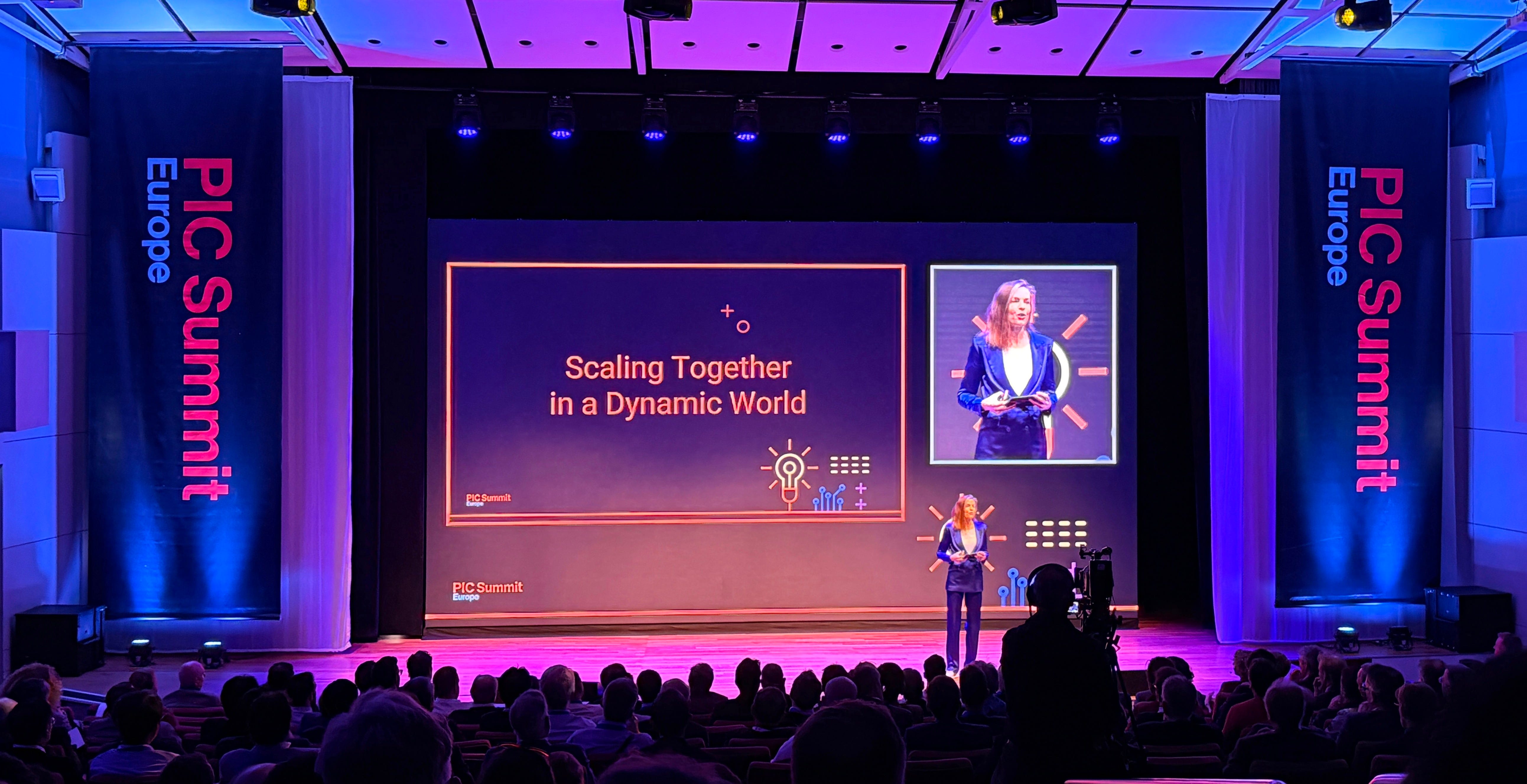
Held every year in Eindhoven, the Netherlands, PIC Summit Europe has become a global barometer for the integrated photonics industry. The 2025 summit, themed “Scaling Together in a Dynamic World,” brought together more than 700 participants from over 20 countries across three days of keynotes, technical forums, and side events. The conference emphasized the pivotal role of photonic chips in next-generation high-performance computing, data centers, metrology, and sensing. It also called for greater collaboration across manufacturing, applications, and investment to meet surging demand.
For Taiwan, integrated photonics is not only about competing in a global technology race—it is also tied to supply-chain restructuring and overcoming AI-era compute bottlenecks. Taiwan holds advantages in semiconductor manufacturing and advanced packaging/testing, while the Netherlands offers strengths in InP, SiN platforms and design ecosystems. Together, the two regions form a naturally complementary partnership that could spark the next major wave of industry growth.

Organized by PhotonDelta, PIC Summit Europe is designed to connect designers, foundries, system integrators, end users, investors, and policy makers. The 2025 edition was held at Evoluon Eindhoven, with its central theme underscoring a critical inflection point: demand is rapidly expanding beyond high-speed communications into AI compute, sensing, and quantum technologies. Without synchronized scaling in manufacturing, standardization, and cross-domain collaboration, many innovations risk stalling before reaching real-world deployment.
The conference program spanned four major domains:
Policy & Ecosystem
Advanced Processes & Materials
Packaging & Heterogeneous Integration
Application Expansion
Key highlights included:
Technical forums on mass production of InP and SiN, heterogeneous integration, and updates on Al₂O₃ and TFLN research.
Advanced packaging and Co-Packaged Optics (CPO) sessions focused on high-bandwidth CPO, shared-laser architectures, and packaging standards.
Application Day, showcasing progress in data centers, high-speed telecom, automotive LiDAR, biomedical sensing, and quantum interconnects.
Policy and Investment discussions on EU Chips Act 2.0, the PIXEurope pilot line, and national support strategies.
The PIC Industry Executive Forum and technical site visits addressing PIXEurope connections and ecosystem coordination.
Taiwan at the PIC Summit 2025
Notably, this year’s summit featured the first dedicated Taiwan session, highlighting rapidly strengthening collaboration between Taiwan and the Netherlands. PhotonDelta has organized multiple delegations to Taiwan since 2023 and has participated actively in SEMICON Taiwan, with the goal of partnering with Taiwanese companies in packaging, automated testing, and heterogeneous integration.
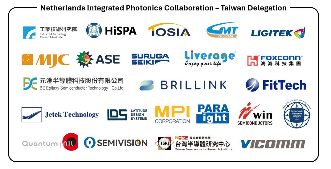
Taiwan’s delegation—coordinated by HiSPA (Heterogeneous Integration Silicon Photonics Research Center), TOSIA (Taiwan Optoelectronic Semiconductor Industry Association), ITRI (Industrial Technology Research Institute ), and the Netherlands Office Taipei —focused on three strategic objectives:
Showcase Taiwan’s strengths in manufacturing and advanced packaging, including OSATs such as ASE and WIN Semiconductors, which are actively expanding photonic packaging capabilities.
Seek complementary collaboration with Dutch design and materials expertise, combining Dutch InP/SiN platforms with Taiwan’s high-volume production capacity to accelerate heterogeneous integration and advanced packaging.
Explore cross-border platforms and talent exchange, strengthening long-term industrial cooperation.
The Taiwan delegation includes representatives from academia, government research institutes, and companies across Taiwan’s semiconductor and photonics industry. This marks the largest participation to date, with members coming from a wide range of organizations. Many of these companies are actively collaborating with Dutch partners to co-develop innovative photonics products and technologies.
Collaboration Prospects Between the Dutch Integrated Photonics Ecosystem and Taiwan
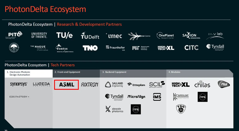
The Netherlands’ integrated photonics ecosystem—anchored by the PhotonDelta alliance—brings together TNO, IMEC NL, Eindhoven University of Technology (TU/e), University of Twente, Delft University of Technology, and a wide portfolio of deep-tech companies and startups. Together, they form one of Europe’s most representative and dynamic photonics innovation networks. The ecosystem traces its roots to the former Philips Optoelectronics Laboratory, where the world’s first compact disc (CD) was invented—an enduring symbol of the Netherlands’ deep heritage in optoelectronics.
PhotonDelta is now actively pursuing a global expansion and supply-chain strategy, with a particular focus on Taiwan’s strengths in high-yield manufacturing, advanced packaging, and test & equipment integration. According to official statements and interviews, PhotonDelta and its ecosystem partners have already visited Taiwan more than three times in the last two years, with the goal of building a cross-border collaboration pipeline spanning wafer fabrication to system assembly.
During PIC Summit Europe 2025, the Taiwanese delegation—over 35 members strong—represented the full breadth of the value chain, including design, light sources, packaging, testing, equipment, and system integration. Key ecosystem associations – TOSIA and HiSPA and research institutions including, ITRI, Hon Hai (Foxconn), TSRI (Taiwan Semiconductor Research Institute) underscoring Taiwan’s potential to become a crucial manufacturing hub for Europe’s photonics industry.
On the technology side, the Netherlands’ R&D activities are centered around IMEC and TNO. IMEC focuses on CMOS integration and scaling, photonic integration for edge AI, UWB, and wireless sensing applications, while TNO’s focus is on integration and packaging. The Photonic Integrated Technology Center (PITC)—a joint effort of TNO, TU/e, and the University of Twente—specializes in metrology, OWC, and biosensing, forming a bridge between fundamental research and industrial deployment.
On the commercialization front, several Dutch startups and design houses are actively seeking Taiwanese partners in manufacturing and advanced packaging:
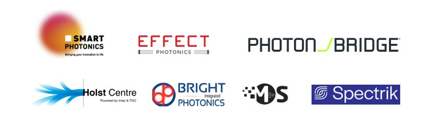
SMART Photonics – Europe’s leading InP wafer foundry, expanding 6-inch capacity with support from TNO and the EU Chips Act, exploring OSAT partnerships in Taiwan for heterogeneous-integration volume production.
EFFECT Photonics – Focused on InP-based coherent communication modules for telecom backbones and data centers.
Photon Bridge – Innovating III-V heterogeneous integration using a cantilever-based bonding approach, achieving 100 nm optical alignment within a 3 μm placement tolerance.
Bright Photonics – Providing multi-platform PIC design services across InP, SiN, LiNbO₃, and polymers; collaborating with TNO on satellite beam-forming modules.
MantiSpectra – A TU/e spin-off developing InP-based ChipSense spectral sensors for wearable health monitoring.
Spectrik – Developing CLDS-based ammonia (NH₃) sensors with a target of 100,000 units per month, aimed at reducing agricultural emissions.
Collectively, these companies demonstrate how Dutch integrated photonics is rapidly advancing from R&D toward scalable manufacturing. Taiwan’s mature ecosystem in wafer-level packaging, testing, and system integration provides the missing industrialization link—turning photonic innovation into deployable, high-volume products.
This partnership is no longer about a simple supply-chain split. It marks the emergence of a new EU–Taiwan co-innovation framework for photonics, where the Netherlands leads in foundational research and design platforms, while Taiwan drives applied innovation, system integration, and global scalability. This model enables PIC technologies to evolve from prototypes into mass-market products powering AI data centers, communication infrastructure, and next-generation sensing.
One can imagine this ecosystem as a “Photonics Lego Mega-Factory”: Dutch innovators produce a diverse inventory of advanced photonic building blocks—such as SMART Photonics’ InP components; design firms like Bright Photonics provide the blueprints; and Taiwan assembles these pieces into real-world, high-performance systems through advanced packaging, testing, and manufacturing.
From AI optical interconnect engines to ultra-sensitive biomedical sensors, this emerging Netherlands–Taiwan photonics partnership is illuminating the technological trajectory of the next decade.
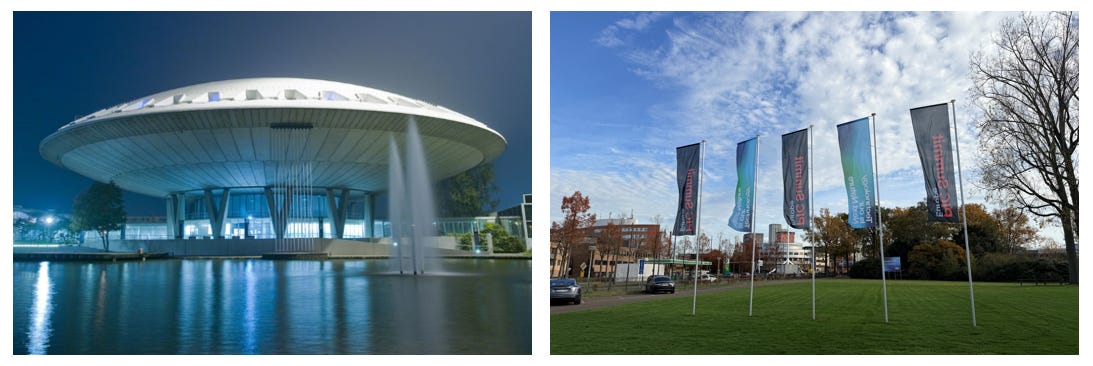
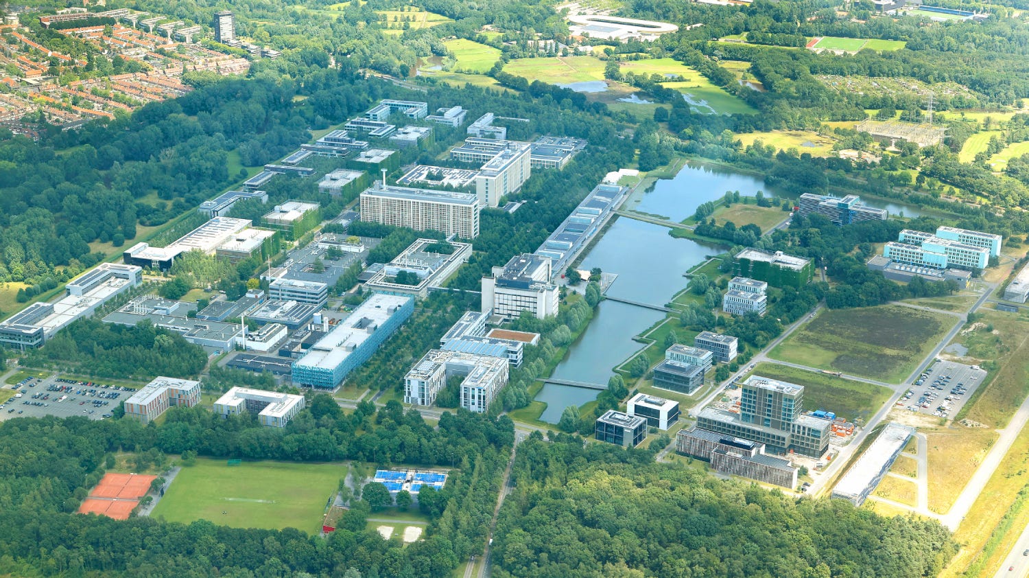
PIC Summit Europe at the Iconic Evoluon in Eindhoven
PIC Summit Europe 2025 was held at Evoluon, the iconic UFO-shaped landmark in Eindhoven originally built by Philips in 1966 to celebrate its 70th anniversary. The building once served as a science museum and convention center, symbolizing the Netherlands’ long-standing legacy in optoelectronics and technological innovation.
The two-day summit featured a dense and content-rich agenda, covering the integrated photonics industry from policy and markets to technology and applications. Below is a day-by-day recap of the key themes, major announcements, and expert insights.
2025 PIC SUMMIT IN Europe : Industry Strategy and Scaling Up
The opening morning set the tone with a dialogue between moderator Irene Rompa and PhotonDelta CEO Eelko Brinkhoff, emphasizing that “scaling manufacturing and expanding applications are equally crucial” to meet the explosive demand for photonic chips in high-performance computing and communications.
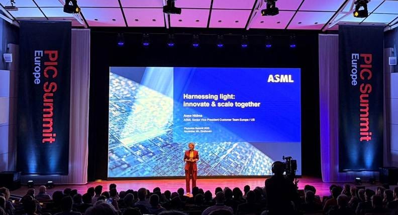
A major highlight followed: Anne Hidma, Senior Vice President at ASML, delivered a keynote on how semiconductor innovation must evolve to meet AI-era compute needs. As a leader in lithography, she stressed that in the post-Moore era, the convergence of photonics and electronics will be essential for sustaining compute performance while reducing energy consumption—aligned with ASML’s vision to support European photonics initiatives.
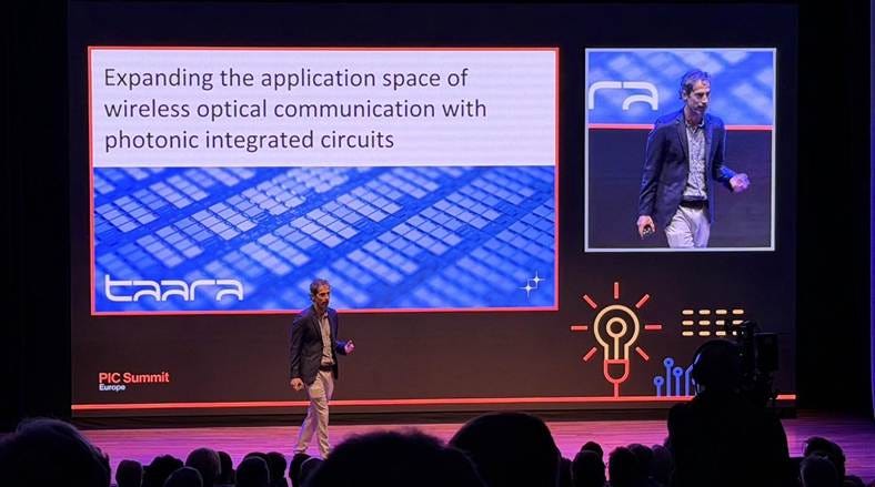
Next, Devin Brinkley, Engineering Director at Taara (under X, formerly Google X), presented a compelling success story: the company is using photonic chips to reinvent terrestrial free-space optical communications, achieving high-rate laser point-to-point links. Originating from the Google Loon project, Taara’s PIC-enabled redesign dramatically shrinks system size while improving reliability, offering a low-cost broadband solution for remote regions.
The session that drew the strongest attention came at the end of the morning: TSMC’s Technical Manager Wen-Chi Chang delivered a keynote titled “Expanding PICs in Europe.” This marked TSMC’s first formal appearance at a major European photonics forum. Chang outlined TSMC’s vision and commitment to integrated photonics, emphasizing Europe’s leadership in research and ecosystem depth. As the world’s leading foundry, TSMC expressed readiness to become a strong partner for Europe’s PIC industry.
His talk focused on industry leadership and emerging technologies: as photonics transitions from lab-scale to industry-scale, accelerating capacity, lowering cost, and transferring advanced manufacturing know-how will be critical. The European audience responded warmly, reflecting strong interest in collaborating with Taiwan to address Europe’s gaps in large-scale manufacturing.
Following TSMC, Gustav Kalbe, Director at the European Commission, highlighted the public sector’s role in driving photonics and quantum innovation. He discussed current EU funding programs and noted that Chips Act 2.0—now in development—will place photonics as a strategic priority, stressing the importance of international collaboration.

A major highlight followed: the introduction of PIXEurope, a pan-European integrated photonics initiative connected to the JePPIX ecosystem and aligned with the broader Chips Joint Undertaking roadmap. Prof. Valerio Pruneri (ICFO), a key leader in European photonics, presented the platform’s vision for scaling design, MPW access, and advanced materials such as TFLN.
PIXEurope consortium to lead the European pilot line on advanced photonic integrated circuits
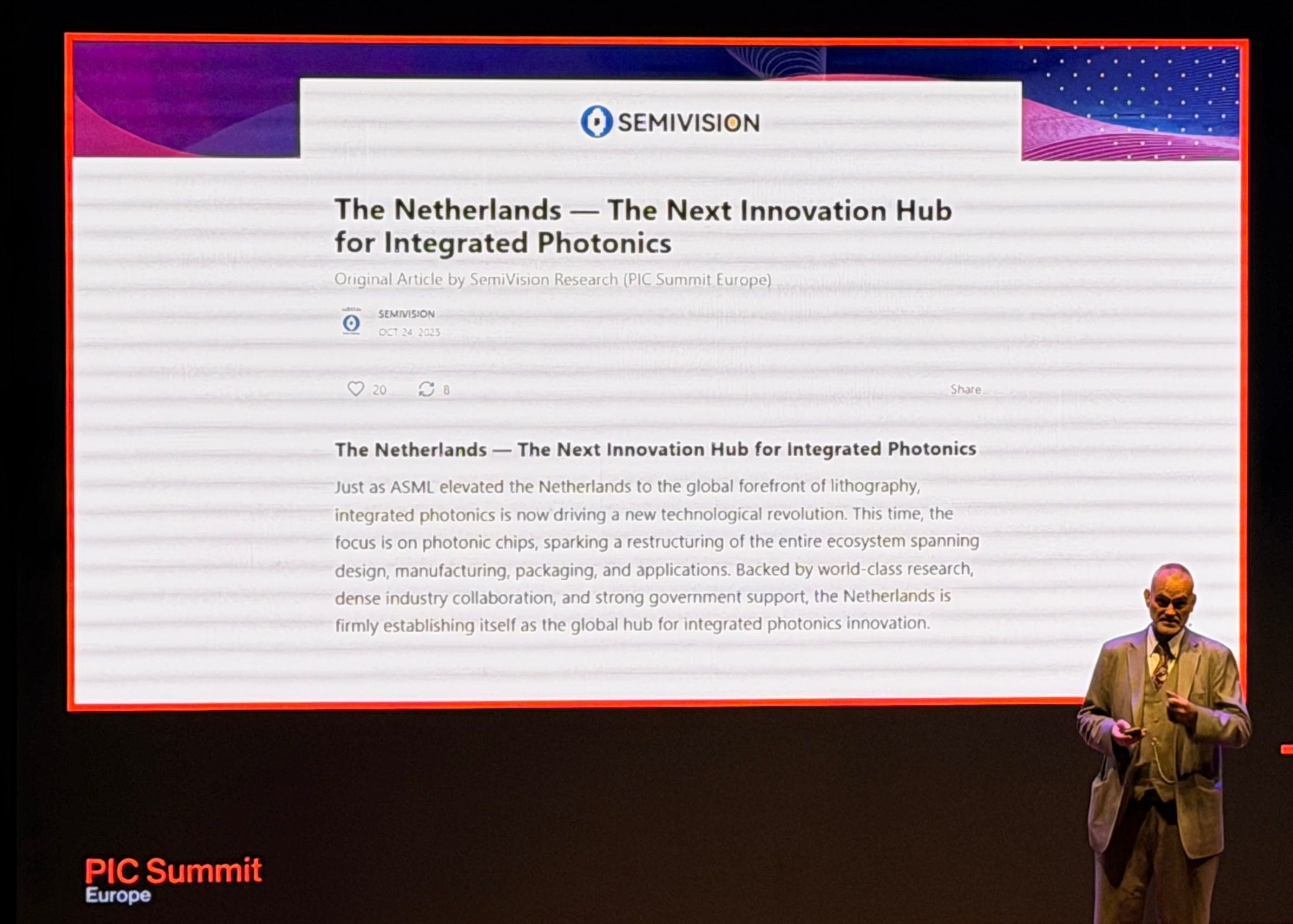
In addition, PIXEurope also referenced SemiVision’s earlier article, and further details can be found in the previous content. The Netherlands — The Next Innovation Hub for Integrated Photonics.

In addition, the Taiwan delegation included representatives from the Hon Hai Research Institute, where Dr. Hao-Chung Kuo delivered a panel talk sharing insights on Taiwan’s latest progress in semiconductor–photonics integration and advanced packaging innovations, highlighting how Taiwan’s ecosystem can collaborate with European partners to accelerate technology commercialization and mass production in the photonics domain.
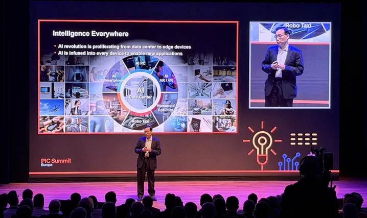
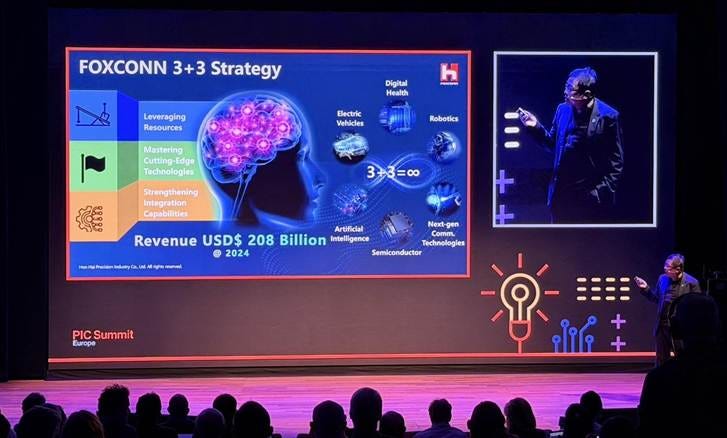
Dr. Hao-Chung Kuo outlined Foxconn’s “3+3 Strategy”—leveraging resources, mastering advanced technologies, and strengthening integration—as the engine behind its growth in EVs, digital health, robotics, AI, next-gen communications, and semiconductors.
He highlighted Foxconn’s shift from component manufacturing to full AI data-centre infrastructure, noting the industry’s move “beyond Moore’s Law” toward Huang’s Law and accelerated GPU-driven compute.
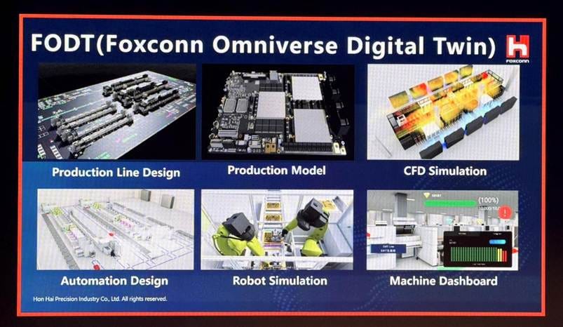
Foxconn’s Omniverse Digital Twin initiative integrates photonics into digital manufacturing, while the company expands R&D in metasurfaces, nanophotonics, and silicon photonics with academic and government partners.
Looking ahead, Dr. Kuo identified InP as a key material for scalable optical performance, and emphasized that while pluggables will remain important, the future of AI data centres will rely on co-packaged optics, heterogeneous integration, and high-bandwidth optical interconnects.

Tower Semiconductor, as one of the world’s leading silicon photonics suppliers, has incorporated Taiwan’s EDA company LDS into its key supply chain, marking an important milestone for Taiwan’s growing role in the global silicon photonics ecosystem. In addition, LDS is actively collaborating with several companies in the Netherlands, making it a significant example of Taiwan–Netherlands cooperation in integrated photonics.

To support this market, Tower is expanding its SiPho platform with complete PDKs that include waveguides, passive components, modulators, and SiGe photodetectors. One of the most important elements in Tower’s strategy is its partnership with Latitude Design Systems (LDS). Tower uses LDS’s PIC Studio to enable fabrication-aware photonic design, automated layout, and co-simulation. PIC Studio integrates directly with Tower’s PDKs, helping customers shorten design cycles and improve manufacturability for high-volume SiPho products.
This design ecosystem strengthens Tower’s broader approach, which includes both monolithic integration with OpenLight (InP lasers + modulators) and hybrid integration models with partners like Cintel. With capacity expansion underway and a growing EDA ecosystem, Tower aims to support the rapid ramp of 800G/1.6T optical modules and future CPO/LPO architectures.
Taiwan at the forefront: Driving global integrated photonics innovation without border
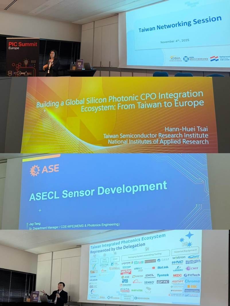
Among the afternoon breakout sessions, the most anticipated was a panel titled “Taiwan at the forefront: Driving global integrated photonics innovation without border” With Taiwan’s large delegation present this year, the summit created a dedicated session for the first time. The discussion was moderated by Prof. San-Liang Lee, Chair of the HiSPA Alliance and professor at NTUST, and featured speakers including Chien-Chung Lin, Division R&D Director at ITRI; Han-Huei Tsai, Deputy Director General of TSRI; Shih-Chieh Tang, Senior Manager at ASE; and Andrew Chen, Deputy Director from WIN Semiconductors’ advanced photonics R&D team.
The panel began with an overview of Taiwan’s emerging integrated photonics ecosystem. Taiwan has built a foundational value chain linking academia, research, and industry—spanning silicon photonics design, III-V epitaxy, wafer processing, and advanced packaging and testing. TSRI and ITRI has launched Silicon Photonics service platform in recent years, OSATs like ASE are advancing photonic packaging capabilities, and WIN Semiconductors—one of the world’s leading compound semiconductor foundries—is developing volume-production processes for InP/GaAs optoelectronic devices.
Panelists emphasized Taiwan’s strengths in advanced manufacturing and supply chain management, combined with the Netherlands’ leadership in photonics design and innovation, form a highly complementary partnership. One speaker noted:
“Taiwan has world-class wafer fabrication and packaging capabilities and is deeply engaged in global collaboration. In communications, healthcare, and AI applications, Taiwan is becoming a key driver of borderless photonic innovation.”
Concrete proposals were also put forward, including:
Establishing cross-border talent exchange programs (European postdocs training in Taiwan’s manufacturing, Taiwanese engineers engaging in frontier research in Europe),
Co-developing interface standards and testing specifications to align both supply chains,
Launching a Taiwan–Netherlands joint MPW program to lower barriers for startups.
Participants broadly agreed that Taiwan and the Netherlands possess complementary strengths in both industrial scale and technological innovation; by joining forces, they can accelerate the global maturation of the photonics industry.
The summit concluded with a session on “Opportunities and Challenges of PICs in Defense and Security.” Representatives from the Netherlands’ TNO, Italy’s Leonardo, and defense contractor Thales discussed applications of PICs in defense communications, sensing (such as radar and fiber-optic gyroscopes), and related fields. Experts noted that military technologies require extreme reliability and wide temperature tolerances—areas where PICs must continue to advance—but in the long term, the advantages in size, weight, and power (SWaP) will drive widespread adoption in defense systems.
With that, the two-day summit came to a close. Across all sessions, it was clear that integrated photonics is rapidly transitioning from laboratory research to broad commercial deployment, with every segment of the value chain accelerating. The exchanges at the summit highlighted a growing trend of collaboration between Europe, Taiwan, and the global photonics community—setting the stage for a much larger and more connected future for the photonics industry.
Expanding Applications and Strengthening Ecosystem Collaboration
The second day of the summit—known as “PIC Application Day”—focused on expanding PIC adoption across diverse verticals and deepening collaboration within the ecosystem.
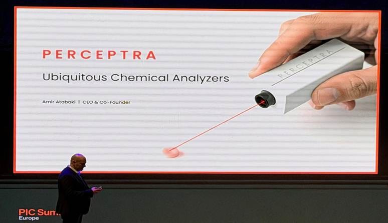
The first session opened with Perceptra, which introduced how the company is applying silicon photonics technology to biomedical sensing. The Perceptra team has developed the world’s first ultra-miniaturized PIC-based Raman spectrometer—1,000× smaller and 100× cheaper than existing systems—capable of real-time molecular analysis. By combining PIC technology with AI, the system can monitor molecular changes in bioprocessing environments, addressing the long-standing bottleneck of slow, expensive laboratory analysis.
During his talk, CEO Amir Atabaki highlighted his research background at MIT, where he worked on monolithic integration of photonics and electronics, enabling optical interconnects and sensing on CMOS platforms. This expertise allowed his team to shrink a laboratory-scale spectrometer into a chip-level device. The presentation drew significant interest from representatives in medical device and pharmaceutical sectors, illustrating the strong potential of PICs in biomedical sensing.
A following fireside chat centered on the theme “PICs Across Diverse Application Domains: Balancing Flexibility and Cost.” Speakers included Joost van Kerkhof, COO of PHIX, and Iñigo Artundo, CEO of VLC Photonics. They discussed how the highly fragmented application landscape of integrated photonics—unlike digital chips concentrated in a few dominant markets—results in a high-mix, low-volume industry today.
Maintaining flexibility while driving down cost under such conditions remains a major challenge. Beyond datacom, each vertical—sensing, healthcare, defense, and others—has vastly different requirements. Panelists emphasized the need for modular, reconfigurable platforms to increase reuse and reduce NRE overhead.
They also cautioned about the varying risks and opportunities across applications: for example, high-margin customized solutions can be attractive but may struggle to reach manufacturable scale, keeping costs high.
The discussion underscored that the PIC industry cannot rely on the traditional semiconductor mindset of “one platform fits all.” Instead, it requires multiple parallel strategies to serve a diverse and expanding set of applications.
Europe’s Strategic Role in Photonics and the Global Race
Integrated Photonics Market Size and Strategic Value
Photonics is more than an industrial sector—it plays a central role in achieving broader policy goals. Even under conservative forecasts, the photonics market is already enormous and is expected to continue expanding.
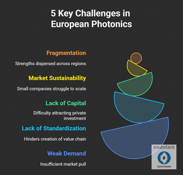
Across multiple high-tech fields, Europe performs exceptionally well in photonics. In certain application domains, Europe is a global leader; in others, it matches the highest international standards. European scientific excellence and industrial capability are well balanced, and Europe’s global market share is broadly aligned with the size of its economy and industrial base.
Photonics is now recognized as one of the core pillars for maintaining and restoring the EU’s competitiveness and technological security. It is essential for high-value markets such as automotive, healthcare, and the rapidly expanding defense sector. Increasingly, photonics is also becoming an enabling technology across a wide set of emerging applications.
Looking ahead, photonics will be deeply integrated—modularly and at scale—with microelectronics and AI processors, forming the backbone of next-generation computing and advanced systems.
SemiVision: The Netherlands — A Next-Generation Hub for Integrated Photonics
The European Commission has praised the Netherlands as a standout model for integrated photonics development—one it hopes to replicate across the EU.
The Dutch model is described as a “highly intelligent approach.”
The ecosystem spans the full chain from fundamental research to innovation, prototyping, component manufacturing, system integration, real-world deployment, startup incubation, and public procurement—resulting in a truly complete, end-to-end photonics ecosystem.
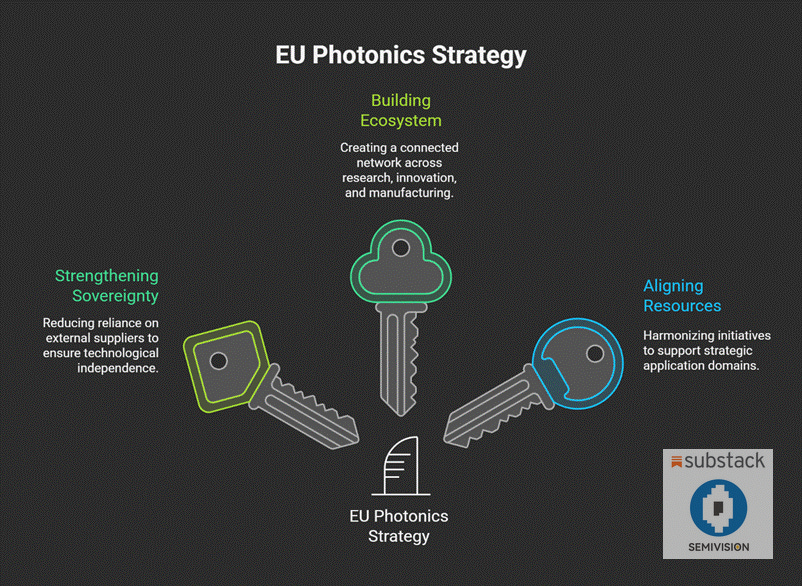
The EU’s objective is not to build isolated or fragmented initiatives, but to create a genuinely interconnected European ecosystem. By distributing centers of excellence across multiple regions and linking them together, the EU aims to strengthen its technological sovereignty while reducing dependence on single choke-points outside Europe.
EU Strategy: Staying Ahead in Global Competition
The EU is now implementing a wide-ranging strategy aimed at safeguarding its competitiveness, security, and independence in the photonics domain. This strategy includes coordinated investment, ecosystem integration, and policy support to ensure Europe remains a leading actor in the global photonics race.
The EU’s core strategy for photonics centers on strengthening technological sovereignty, building an interconnected ecosystem, and aligning all policy instruments to support strategic industries. At the highest level, Europe aims to reduce dependence on non-EU suppliers by mastering and manufacturing essential technologies domestically while establishing a full life-cycle ecosystem supported by shared roadmaps and coordinated tools. To accelerate this shift, the EU is integrating its diverse programs—fundamental research, innovation initiatives, and public procurement—into a unified industrial strategy designed to create globally competitive champions. A crucial pillar of this strategy is leveraging demand-side power: policymakers are exploring consolidated public procurement, including a potential “Buy European” approach, to aggregate demand across sectors such as healthcare, where thousands of hospitals require similar equipment. Such concentrated purchasing would create a large, stable market that lowers investment risks and encourages scale-up of manufacturing capacity.
Looking forward, the EU no longer treats photonics as a standalone sector but as a foundational asset for broader policy goals. Photonics underpins AI supercomputers and emerging quantum technologies, both of which require enormous numbers of photonic components. Without secure access to these components, Europe risks dependency and potential exclusion from the most advanced technologies. As a result, the EU is examining how to integrate photonics more deeply into data-processing architectures and physical infrastructure while preparing the next multi-year financial framework, including the upcoming “Chips 2.0” legislation, which explicitly incorporates photonics. In essence, Europe sees photonics as the structural foundation of a technological skyscraper—essential, strategic, and something it must firmly control to safeguard competitiveness and long-term technological autonomy.
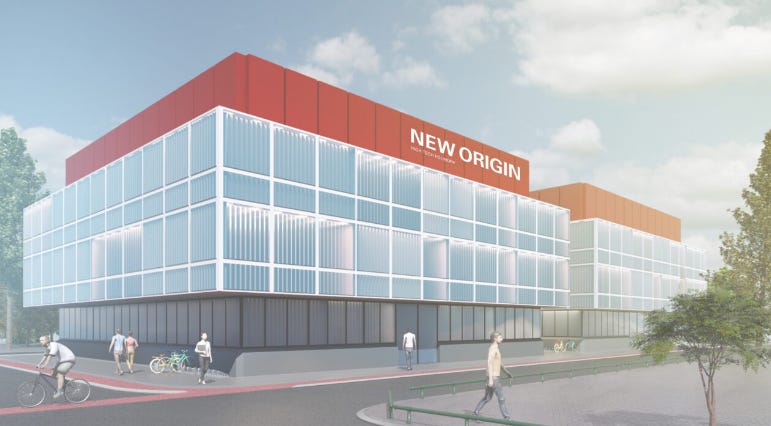
As the world accelerates its shift from electronics to photonics, PIC Summit Europe has become the most influential annual gathering for Photonic Integrated Circuits (PICs). It is not only a stage for showcasing technology but also a strategic focal point for Europe’s high-tech industrial ambitions. Last year, Trumpf announced the creation of New Origin, launching a new pure-play photonic foundry built on a silicon nitride (SiN) platform—symbolizing Europe’s transition from research to scalable manufacturing in integrated photonics.
This year, the spotlight moved to Eindhoven, where a major milestone was unveiled: the launch of a new pilot production line that is poised to become a critical engine for Europe’s photonics manufacturing capacity.
The line is part of the PIX Europe program, funded by the EU Chips Act and supported by PhotonDelta, TNO, the Dutch Ministry of Economic Affairs, and the Dutch Ministry of Defense. Its mission is clear: bring photonics from the lab into the fab, completing the final stretch toward full industrialization.
Located in the heart of the High-Tech Campus (HTC)—celebrated as “the smartest square kilometer in Europe”—the facility will house 2,200 m² of cleanroom space dedicated to front-end processing of indium phosphide (InP). Built on a 6-inch wafer platform, the pilot line is expected to reach an annual capacity of 10,000 wafers, enabling next-generation photonic solutions for data communications, healthcare, and automotive systems.
This infrastructure will serve as both a manufacturing milestone for European photonics and a critical bridge for startups and scale-ups—helping them transition from prototyping to first commercial production batches.
When the cleanroom comes online in May 2027, it will mark the beginning of a new chapter for Europe: an era defined by autonomous and scalable photonic manufacturing capacity.
PIXEurope : Integrated Photonics For Key Application Areas
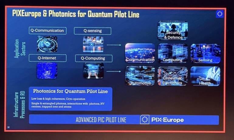
PIX Europe’s technology platform and research activities target multiple strategic sectors, many of which require tight co-integration of photonics and electronics.
If Europe’s photonics industry were an orchestra, PIX Europe would be both the training academy and the instrument workshop. It provides the finest instruments (advanced material platforms), trains future musicians (designers and startups), and helps them compose sophisticated scores (PDKs and technology roadmaps). But when the music (products) is ready, large concert halls (commercial manufacturers) perform the full production, ensuring Europe continues creating world-class technological “music.”
The Taiwanese delegation brings a fully developed semiconductor and optoelectronic ecosystem—spanning design, manufacturing, packaging, and testing.
As the AI era accelerates, photonic integration, particularly silicon photonics, has emerged as a new strategic focus for Taiwan’s technology industry. Our goal at this summit is to share experience with our Dutch partners, co-innovate, scale together, and help elevate photonics into the next global driving force.
As one of Taiwan’s leading research institutions, the Industrial Technology Research Institute (ITRI) has long been dedicated to high-speed chip interconnects and optoelectronic integration, identifying silicon photonics as a critical technology for next-generation data centers and AI systems. ITRI sees two primary pathways for photonic integration: Micro-LED–based solutions and silicon-photonics–based platforms, the latter being fundamental to Co-Packaged Optics (CPO) and ultra-high-speed interconnects. Its silicon photonics initiatives focus on three pillars: photonic integrated packaging, ultra-high-speed chip design, and high-speed/low-loss materials, with the aim of building a comprehensive optoelectronic ecosystem through cross-disciplinary collaboration.
On the technical front, ITRI’s research spans packaging architecture, active and passive device development, and full-flow silicon photonics platform implementation. In packaging, ITRI focuses on PIC–EIC stacking, fiber-coupling strategies, and optimizing signal integrity and system-level performance. In device development, its work includes multi-channel WDM chip design and performance optimization of key components such as Mach–Zehnder modulators (MZMs), surface gratings, and photodetectors. ITRI is also developing a complete silicon photonics process chain covering design, layout, tape-out, PDK development, integration testing, and packaging validation—laying the groundwork for commercial-scale SiPh manufacturing.
Looking forward, ITRI is advancing toward 1.6 Tbps to 3.2 Tbps packaging platforms and building a high-frequency testbed supporting 200G–400G per lane. After upgrades are completed in 2026, this platform will be opened to industry partners as a key validation hub for photonic technologies. ITRI emphasizes that the success of high-speed interconnects depends on chip design and I/O packaging integration—areas where the institute already has strong technical foundations and production support.
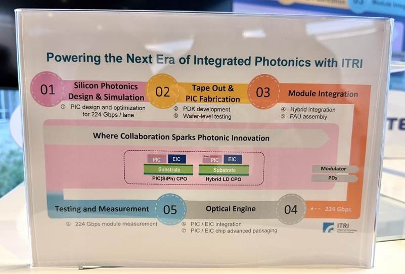
In terms of international collaboration, ITRI sees Taiwan’s complete supply chain—from design, manufacturing, packaging, testing, to materials and equipment—as highly complementary to the Netherlands’ strengths in photonics design, process innovation, and materials research. Through cooperation in platform co-development, test services, and heterogeneous integration packaging, the two sides can accelerate industrial adoption of CPO and next-generation optoelectronic architectures. Overall, ITRI showcases Taiwan’s systematic deployment in silicon photonics while opening new opportunities for Taiwan–Netherlands collaboration—from joint R&D to full industry-level partnerships.
III-V Compond Leading Company : WIN Semiconductor

WIN Semiconductors is Taiwan’s leading III-V compound semiconductor foundry, specializing in GaAs, GaN, and InP processes. Within the silicon photonics landscape, WIN positions itself as a critical manufacturing platform for high-performance light sources and active devices. The company sees itself playing two core roles in the global PIC ecosystem:
supplying III-V devices for silicon-photonics applications—such as saturable absorbers and laser diodes;
advancing monolithic InP PIC manufacturing, integrating active and passive components on a single InP chip.
WIN showcased a high-power open-cavity DFB laser capable of delivering over 100 mW at 75°C and 300 mA, demonstrating excellent high-temperature performance. The company also develops essential components such as electro-absorption modulators (EAMs), Mach–Zehnder modulators (MZMs), and photodiodes (PDs). With existing 6-inch foundry capacity, WIN notes that if InP epitaxy expands to 6-inch wafers in the future, production throughput could scale rapidly to support volume manufacturing.
WIN is also developing monolithic InP PICs, combining lasers, modulators, and detectors on one chip to achieve low insertion loss and wide bandwidth. However, InP technology still faces challenges: high material cost, lower integration density, complex processing, and weaker cost competitiveness compared with silicon photonics, especially at large manufacturing scale. To address this, WIN adopts a technology-provider strategy, offering custom process modules tailored to client needs rather than providing a universal PDK—maintaining flexibility and differentiation.
At the industry level, WIN observes that the III-V photonics ecosystem remains less mature than the silicon-photonics ecosystem. The sector must confront strong competition from vertically integrated device manufacturers (e.g., Lumentum, Coherent), and standardized PDK development remains difficult. WIN argues that the industry should advance through specialized division of labor and deep collaboration: design houses and prototyping labs drive innovation and verification, while foundries like WIN focus on scalable production and commercialization.
In terms of international collaboration, WIN highlighted the complementary differences between its process technologies and those of SMART Photonics in the Netherlands. WIN uses electron-beam lithography (EBL) for design flexibility, while SMART Photonics employs DUV lithography for higher throughput and standardized manufacturing. These differences create a natural alignment for Taiwan–Netherlands cooperation in the InP domain. By sharing process expertise, co-developing process modules, and standardizing manufacturing flows, both sides can accelerate the convergence and industrialization of InP and silicon-photonic technologies.
Overall, WIN Semiconductors serves as the “engine manufacturer” of the photonics industry—delivering high-performance III-V light sources to power silicon photonics, while pushing InP platforms toward scalable manufacturing. As Taiwan and the Netherlands deepen collaboration across design, processing, and packaging, the global photonic-integration ecosystem will grow stronger, paving the way for a more efficient and economically scalable photonic era.
Leading Package Company ASE:
ASE’s MEMS & Photonics Engineering (MPE) division serves as the company’s core team for sensors, optical MEMS, co-packaged optics (CPO), and silicon photonics (SiPh). Comprising roughly 30 experts, the group develops optical sensors, MEMS devices, and SiPh technologies. ASE views packaging as the key differentiator for sensors and photonic components—more than just a bridge between the electronic and optical domains, packaging is essential for achieving performance stability and scalable high-volume manufacturing. The MPE team has world-leading mass-production experience, already shipping qualified products, and maintains a complete laboratory infrastructure covering stress, thermal, fluidic, and material simulations, along with an in-house materials database for independent package validation and failure analysis.
In silicon photonics and CPO, ASE sees its next major growth engine. The company is already collaborating with multiple customers on optical engines and demo platforms, covering 400G to 1.6T transceivers, coherent modules, and multimode/single-mode VCSEL arrays. Technically, ASE has built a comprehensive manufacturing flow through its internally developed “Toolbox” strategy, spanning wafer-level optical probing, laser integration, and PCB assembly. It is also advancing several innovative packaging technologies, including high-reliability nano-twin copper (NT-Cu), low-temperature/low-pressure Copper Prime bonding (150°C, 2 MPa), and UTS ultra-thin-substrate solutions. These innovations improve both performance and energy efficiency while aligning with broader ESG trends.
For optical alignment, ASE emphasizes passive alignment as the core approach, combined with detachable fibers and multiple coupling architectures (edge and surface coupling) to ensure scalability and process stability. The team also conducts research on in-house laser module fabrication and direct bonding to PICs, laying the groundwork for tightly integrated photonic engines. Looking ahead, ASE is extending its silicon photonics platform into emerging domains such as LiDAR (FMCW), biophotonics, optical I/O (OIO), and AI photonic computing, creating a unified technology chain that spans sensing and computation.
ASE’s long-term vision is embodied in its APRIL platform (Advanced Photonic Reconfigurable IsLand)—a reconfigurable, multifunctional photonic integration architecture that combines silicon photonics, optical MEMS, and advanced packaging. The platform aims to support diverse applications such as spectroscopy, optical microphones, accelerometers, LiDAR light sources, and plasmonic filters. If ASE’s photonics roadmap is compared to a massive “silicon-photonics vessel,” then the packaging and materials technologies of the MPE team are its engine and fuel—delivering innovative interconnect structures and high-reliability packaging to provide the high-performance, low-cost, and scalable industrial capacity required for the rapidly growing SiPh market, while driving the convergence of AI, CPO, and sensing applications.

LIGITEK Launches 3.2T High-Speed Optical Module Program: Targeting the Next-Generation AI Datacenter Interconnect Market
As AI and high-performance computing workloads surge, the bottleneck inside datacenters is shifting from compute to two critical constraints: bandwidth and power efficiency. In response, LIGITEK is moving aggressively into high-speed optical communications, partnering with Liverage and Dutch ecosystem players to jointly advance a “3.2T Silicon Photonics Optical Module Program,” aimed squarely at next-generation optical transceiver markets.
This initiative centers on Silicon Photonics integration, with the goal of building high-bandwidth optical modules capable of supporting AI datacenters and supercomputing platforms. The “3.2T” specification represents 3.2 terabits per second, four times the throughput of today’s mainstream 800G optical modules. By integrating multi-channel modulators, photodetectors, and driver circuits onto a single chip, the module targets ultra-high density, low-power, fully scalable optical transceiver architectures.
LIGITEK’s role is to extend its deep experience in electronic manufacturing and modular integration into the electro-optical domain, establishing a 3.2T optical platform with strong manufacturability and reliability. Liverage contributes advanced optical-module packaging and system-level testing, while the Dutch partners provide InP and SiN process technologies, reinforcing capabilities in photonic integration and heterogeneous bonding.
Notably, this 3.2T module aligns with the core direction of the high-speed optical transceiver (TR) market. AI clusters and datacenter switches are rapidly transitioning to 3.2T / 6.4T optical modules, replacing copper interconnects and enabling emerging CPO (Co-Packaged Optics) and LPO (Linear Pluggable Optics) architectures. LIGITEK’s move signals a strategic evolution for Taiwan: transitioning from traditional PCB and electronic module manufacturing toward advanced photonic-integrated, packaging-centric system development.
This program is also seen as a flagship project of the Taiwan–Netherlands Photonics Alliance, supported by ITRI and national-level R&D organizations. It represents not just a business collaboration, but a milestone in Taiwan’s entry into the “Electronics × Photonics” era.
If the 3.2T module achieves successful TR sample development and system validation, it could soon be deployed in AI servers, switching platforms, and hyperscale datacenters—becoming a key enabler for next-generation high-speed interconnects and electro-optical integration.
Thin-Film Lithium Niobate (TFLN) in 400G and Beyond
A Complete Overview of Its Role in Next-Generation Optical Interconnects—Materials, Processes, Platforms, and Industrialization

As global data consumption grows a thousand-fold over a decade and compute continues to outpace interconnect speeds, the real bottleneck in data centers has shifted from compute to the interconnect and memory wall. To unlock the performance of GPUs and AI accelerators, optical interconnects have become indispensable. Within current 400G production nodes—and with 800G/1.6T accelerating toward deployment—Thin-Film Lithium Niobate (TFLN) has emerged as one of the most certain high-speed electro-optic platforms.
Why TFLN: A Triple Advantage from Physics to System Architecture
Ultra-high electro-optic response (>100 GHz)
The Pockels (linear electro-optic) effect enables instantaneous refractive-index modulation. The intrinsic response time of the crystal is on the femtosecond scale, meaning driver and electrode design—not the material—define the bandwidth limit. Production-grade TFLN modulators have demonstrated 100–110 GHz 3 dB electro-optic bandwidth, supporting 400G PAM4 and 800G (4×200G) transceiver topologies, while paving the path to >100 Gbaud coherent and direct-detect transmission.High thermal stability and long-term reliability
TFLN is a ferroelectric material with a Curie temperature above 1000°C, giving it a wide process and operating window. High-temperature tuning (up to ~400°C) can optimize waveguide and RF phase matching, resulting in more stable bandwidth and insertion-loss performance under controlled thermal operation.Low propagation loss and wide transparency window
TFLN can achieve ultra-low-loss waveguides (typically <1 dB/cm; state-of-the-art processes reach few dB/m), reducing DSP burden and power draw. Its broad transparency window spans C/L/S bands and beyond, supporting dense WDM scaling and enabling nonlinear functions such as frequency conversion and optical sampling.The 400G → 800G/1.6T Transition: Why TFLN Is Especially Critical
Today’s hyperscale data centers rely on 400G pluggable optics. Scaling to 800G/1.6T requires 200G-class lanes, which demand >100 GHz modulator bandwidths and improved electro-optic efficiency (BW·Vπ·L). Higher baud rates (>100 Gbaud) and reduced drive voltage (Vπ) cut power and mitigate electrical losses.
In CPO/OIO and high-density optical I/O architectures, link lengths shrink while crosstalk and thermal density rise, increasing reliance on high-frequency, low-loss, thermally stable EO platforms. TFLN’s material attributes fit this system requirement precisely.
Platformization and Manufacturing: From Materials Innovation to 200 mm High-Volume Capability
To establish TFLN as a long-term, reusable industrial platform, the ecosystem must advance across design, fabrication, packaging, testing, and supply chain.
1. 200 mm wafer-scale production and supply chain
Leading suppliers now provide high-yield, high-uniformity TFLN processes on 200 mm wafers, with monthly capacity reaching ~1000 wafers—sufficient for Telecom/Datacom applications. Foundry services support MPW shuttles and full PDKs (passive/thermal/RF/electro-optic libraries), with full-size 25×33 mm DUV reticles and mature ~110 nm critical-dimension process flows.
2. Design toolchains and modular PDKs
PDKs typically include low-loss waveguides, grating/edge couplers, thermo-optic modulators, RF electrodes, phase/amplitude shifters, and IQ modulators. Electro-optic/RF co-design and thermo–mechanical–electrical co-simulation shorten design cycles and support >100 GHz co-packaged design.
3. Packaging and test readiness
Packaging services now support ~110 GHz RF electro-optic testing, enabling validation of 400G/800G prototypes and engineering builds. Wafer-level probing (WLP) and module-level test capabilities complete the design–fab–package–test closed-loop flow.
4. Material Comparison and Selection: Choosing Between InP, Si, SiN, and TFLN
InP excels at active functions such as light generation and photodetection, while Si and SiN are well suited for low-loss passive routing and large-scale integration. TFLN, in contrast, offers a high-speed, low-Vπ electro-optic modulation platform. Heterogeneous integration allows each material to be deployed where it performs best, achieving system-level optimization across performance, cost, and scalability.
5. System Design Requirements: Scaling from 400G to 1.6T / 3.2T
As baud rates rise beyond 100 Gbaud, modulators must deliver >100 GHz EO bandwidth while maintaining low Vπ·L and proper RF impedance matching. TFLN’s low drive voltage and high electro-optic efficiency directly reduce power consumption, helping keep pJ/bit metrics within practical limits at 800G/1.6T. Its high-frequency, low-loss, and phase-stable behavior also simplifies the design and testing of dense optical modules.
6. Manufacturing and High-Volume Considerations
TFLN development today focuses on three pillars: EO modulation, strong nonlinear optics, and ultra-low-loss waveguides. The 200 mm PIC process flow and MPW shuttles are now accessible, PDK ecosystems are maturing, and packaging/test capabilities support up to ~110 GHz. Future challenges include light-source integration and high-power reliability, >100 GHz driver chains, and long-term stability under thermo-mechanical-electrical coupling.
7. Engineering Recommendations
Modulator design should leverage travelling-wave electrodes (TWE) and RF co-design to minimize loss and reflections. For heterogeneous integration, a TFLN modulation core can be combined with InP light sources/PDs and Si/SiN passive waveguides. In CPO/OIO architectures, passive alignment and precision packaging must be strengthened, and a unified verification flow—from wafer-level to module-level—should be built using 110 GHz measurement platforms.
Equipping Optical Interconnects with a TFLN “Jet Engine”

Europe’s leadership in thin-film lithium niobate (TFLN) is not accidental; it is the product of a long, coordinated, and multi-layered effort across materials science, industrial capability, academic excellence, and strategic EU investment. The region began investing in lithium niobate research much earlier than most of the world, with institutions like ICFO, CEA-Leti, and IXblue advancing foundational LN materials science more than a decade ago. This early start allowed Europe to become one of the first regions to push wafer-scale bonding, hybrid integration, and high-yield thin-film processes, efforts led by groups such as Leti and LioniX, who helped transform TFLN from a lab-scale material into a manufacturable platform. At the industrial level, Europe benefits from a uniquely mature LN applications ecosystem, with IXblue standing as one of the global leaders in LN modulators and specialty components. This industrial depth is matched by an exceptionally strong academic network—TU/e, the University of Twente, EPFL, and Fraunhofer—whose research output continues to expand the boundaries of EO bandwidth, low-loss waveguides, and nonlinear photonics. Finally, Europe’s ability to execute continent-wide programs such as H2020, Horizon Europe and Chips JU has accelerated chip-scale LN development, uniting universities, foundries, equipment makers, and system companies under shared roadmaps and funding. Taken together, these advantages explain why Europe holds a uniquely powerful position in the global TFLN landscape, and why the region is now shaping the next era of high-speed electro-optic integration.

This year’s PIC Summit Europe made one point especially clear: TFLN represents a major collaboration opportunity between Europe’s photonics ecosystem and Taiwan’s semiconductor industry. Europe has spent more than a decade building early expertise in TFLN materials science, thin-film processing, and academic research, giving it a strong technological head start. Taiwan, despite its world-class manufacturing and packaging capabilities, is still in the early stages of understanding and engaging with this material platform. This gap creates a natural complementarity. By combining Europe’s deep R&D foundation with Taiwan’s scale manufacturing, system integration, and supply-chain strengths, TFLN could become a powerful new pillar for joint innovation in next-generation optical interconnects and silicon photonics.
As compute curves continue to surge upward, interconnects must evolve in lockstep as the system’s transmission backbone. With demonstrated >100 GHz bandwidth, low-loss waveguides, exceptional thermal stability, and a maturing 200 mm manufacturing and PDK ecosystem, TFLN offers the industry a practical, scalable, and sustainable electro-optic platform for the 400G and 800G/1.6T transition. Looking ahead to the 1.6T/3.2T era—defined by higher baud rates, tighter packaging, and greater thermal density—the heterogeneous combination of TFLN + InP (light sources/PDs) + Si/SiN (low-loss passives) will become the mainstream architecture linking Datacom/Telecom networks with AI data centers. Using the right material for the right function is the shortest and most reliable path toward the Zetta-scale future.

Several startups and research institutes are now accelerating development on the TFLN platform. One example is CCRAFT, a spin-off from Switzerland’s CSEM, which announced in 2025 that it can already support MPW (multi-project wafer) runs on 6-inch LNOI wafers, in partnership with Soitec to secure a fully European supply of LNOI substrates. The EU ELENA program also produced the first European-made LNOI wafers in 2025, marking a milestone in establishing a domestic supply chain. Since high-quality LN wafers were historically sourced from one major non-EU supplier, this shift toward European production is expected to accelerate ecosystem maturity. CCRAFT plans two MPW runs in the second half of 2025, starting with C-band processes and later expanding to O-band (Datacom) and visible/quantum wavelengths.
Looking ahead, the first major commercial market for TFLN photonic chips is high-speed optical interconnects and AI datacenter acceleration. The industry expects rising demand for 800 Gbps to 1.6 Tbps optical links in AI clusters to drive TFLN PIC commercialization. Meanwhile, lithium niobate’s broad transparency window and strong nonlinear properties position it well for precision sensing (such as LiDAR) and quantum information applications (such as quantum frequency conversion and entanglement generation).
The current bottleneck remains wafer supply and manufacturing capacity: high-quality large-diameter LNOI wafers are still in shortage, and thin-film bonding plus fabrication workflows continue to move toward standardization. To address this, industry players are aggressively expanding capacity. CCRAFT, for instance, aims to reach several million TFLN chips per year by 2028. As the supply chain matures and process standards strengthen, TFLN is poised to become the next major high-speed photonics platform following silicon photonics.
New Material Innovations in Integrated Photonic : AIOx
Aluminum oxide (AlOₓ) has emerged as a highly stable and versatile photonic material that strengthens silicon-based photonic platforms thanks to its optical performance and process compatibility.
AlOₓ offers an exceptionally wide transparency window—from the ultraviolet (UV) through the mid-infrared (mid-IR)—with losses of only a few dB per meter at telecom wavelengths (1550 nm). Even in the 260–300 nm UV range, it maintains propagation losses around 4 dB/cm. Its high linearity and low nonlinear absorption allow it to sustain extremely high optical power, with peak levels reaching up to 800 W without significant thermal effects or multiphoton absorption. The material’s moderate refractive index enables efficient fiber-mode matching, and its deposition via reactive ion sputtering (RIBS) supports wafer-scale, high-volume manufacturing with strong process scalability.

Critically, AlOₓ also exhibits very high rare-earth solubility, enabling doping with elements such as erbium (Er) or samarium (Sm) to create on-chip optical amplifiers and laser-gain structures. Er-doped AlOₓ, for instance, can deliver amplification gains of up to 24 dB at 1550 nm. When integrated with silicon nitride (SiN), a hybrid platform emerges in which SiN provides ultra-low-loss routing and wavelength-division functionality, while doped AlOₓ layers supply optical gain—combining low-loss passives with active amplification on a single chip.
In terms of applications, AlOₓ supports not only telecom and datacenter optical amplifiers but also extends into UV photonics such as ion-trap quantum computing, UV spectroscopy, biomedical sensing, and OCT (optical coherence tomography) imaging chips. With its broadband transparency, low loss, high-power handling, and dopable gain characteristics, AlOₓ has become a foundational material in the silicon photonics ecosystem. It functions like the “Swiss Army knife” of photonics—flexible, stable, and seamlessly integrable—laying the groundwork for next-generation high-power, broadband, and hybrid optoelectronic technologies.
Advanced Packaging and Co-Packaged Optics Issues
Challenges, Standardization Progress, and Taiwan–Netherlands Collaboration Opportunities
As photonic chips advance toward higher bandwidth and higher integration, advanced packaging and co-packaged optics (CPO) are becoming critical bottlenecks and major R&D priorities. Many experts at the summit stressed that “even the best photonic chip is useless without reliable packaging—without packaging, you have nothing.” One of the biggest challenges in integrated photonics today is establishing a complete, dependable ecosystem that supports every step from chip design to final packaging.
Packaging and ecosystem challenges:
PHIX CEO Albert Hasper emphasized that design tools and manufacturing workflows in the photonic chip industry are still immature. Shipments remain low, making it difficult for customers to trust long-term supply stability. Many photonic component PDKs are still at an early stage and lack the extensive, well-validated building-block libraries common in mature semiconductor platforms. “The entire ecosystem must grow to a level where customers can truly trust it,” he said.
Hasper also pointed out that while the EU Chips Act is directing massive investment toward front-end semiconductor manufacturing, Europe still relies heavily on Asia for back-end packaging—leaving a major gap in the photonics supply chain. Even if TSMC eventually builds fabs in Europe, the photonics industry will remain incomplete without parallel investments in advanced packaging. As photonic modules become increasingly complex—especially with heterogeneous multi-chip integration—the European industry is realizing the urgency of upgrading packaging capabilities.
He expects major OSATs (such as ASE and Amkor) to incorporate heterogeneous photonic packaging into their roadmaps. European companies like PHIX have already developed key processes such as fiber-array coupling and automated alignment, and could collaborate with these OSAT giants to address volume-manufacturing challenges. Hasper highlighted that ramping from medium-scale production to high-volume manufacturing remains Europe’s weak spot, and collaboration with Taiwan is a strong opportunity. As he put it:
“We know very well we cannot do this alone. We must work with Taiwan and global partners to make this industry mature and operational.”
This is why in 2023, 2024 and 2025, PhotonDelta coordinated a delegation of Dutch companies—including SMART Photonics (InP foundry), PHIX (photonics packaging), and research institutes such as TU Eindhoven and the University of Twente—to visit Taiwan during SEMICON Taiwan, focusing on advanced packaging, heterogeneous integration, and supply-chain collaboration. The message is clear: the Netherlands sees Taiwan’s semiconductor manufacturing and packaging expertise as essential to accelerating photonic-chip industrialization.
Co-Packaged Optics (CPO) and Optical I/O:
In high-performance computing and datacenter applications, electrical interconnects face increasing limitations in power and bandwidth. CPO has therefore become a key breakthrough. CPO integrates the optical engine directly inside the processor or switch package, replacing pluggable optical modules and significantly shortening the electrical path. This reduces power consumption and latency while supporting higher port counts (high radix).
Several talks at the summit focused on standardization and progress in CPO. Dr. Hao-Chung Kuo, Director of the Semiconductor Center at Hon Hai Research Institute, shared Taiwan’s latest advances in AI datacenter CPO. His team has built a full workflow from device simulation, chip fabrication, advanced packaging, to testing. Using thin-film lithium niobate (TFLN) and organic polymers, they developed hybrid Si-based modulators targeting >200 Gbps per channel. Recent PAM4 tests showed TDECQ around 1.6 dB, demonstrating excellent performance. The team is also developing DFB-laser arrays for 3.2 Tb/s WDM systems and photonic-crystal-laser metasurface integration for sensing and optical communication. These innovations, backed by papers and patents, highlight Taiwan’s growing R&D strength in CPO.
InP Platform: Process and Device Evolution for Datacenters and Quantum Communications
Indium phosphide (InP) is one of the longest-standing PIC material platforms. Since the first InP laser-modulator chip in the 1980s, it has continuously pushed integration density. Its direct bandgap allows it to both guide and generate light, enabling lasers, modulators, and amplifiers to be monolithically integrated on the same chip—something silicon and silicon nitride cannot do. PhotonDelta CFO Laurens Weers noted:
“Silicon cannot emit light; if you need an active laser, you must introduce other materials. InP is the natural choice.”
InP remains the dominant platform for optical communication, powering everything from backbone networks to datacenter transceivers. InP components cover O-band and C-band and have already demonstrated >100 Gbps operation, with research pushing toward even higher baud rates. Dutch foundry SMART Photonics supports large-scale InP PIC manufacturing, and research is progressing on InP-on-Si epitaxy for tighter integration with silicon photonics.
Applications span long-haul coherent communications, hyperscale datacenter optics, FTTH broadband, 5G fronthaul, automotive LiDAR, environmental sensing, and quantum communications. For instance, EFFECT Photonics integrates tunable lasers, modulators, and receivers on InP for 5G and datacenter modules, while InP-based quantum random-number generators and CV-QKD transmitters have also been demonstrated. A notable breakthrough came in 2025 when a photonic-microcomb-driven 100 GHz clock chip was developed, two orders of magnitude faster than electronic clocks, potentially transforming AI computing—though stability and packaging remain challenges.
SiN Platform: Ultra-Low Loss and Wide-Spectrum Applications in LiDAR and Sensing
While silicon and SiN are both mainstream PIC platforms, SiN offers major advantages in ultra-low loss and broadband transparency. SiN is transparent from ~400 nm visible light to ~2.3 µm, covering telecom plus visible wavelengths essential for biophotonics, diagnostics, microscopy, and AR/VR. Dutch startup Surfix Diagnostics built a low-cost disposable SiN biosensing chip using LioniX’s SiN platform, enabling handheld cancer screening. LioniX is also applying SiN to visible-light integrated lasers for AR glasses.
SiN’s hallmark is ultra-low propagation loss—down to 0.01 dB/cm in commercial platforms and 0.0001 dB/cm in research. This enables large-scale interferometric circuits and long optical paths. QuiX Quantum’s processors rely on LioniX’s TriPleX SiN platform to preserve quantum coherence across huge optical networks.
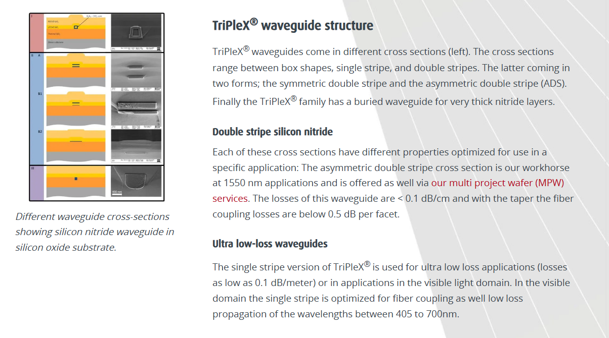
SiN also supports very high optical power, reaching tens of watts in visible wavelengths and >100 W in infrared, far surpassing Si and InP. This makes it ideal for LiDAR, projection, security scanning, and high-power illumination. For automotive FMCW LiDAR, SiN supports long-distance, high-resolution sensing.
However, SiN is a passive platform; it cannot integrate lasers or high-speed modulators. Thus it must be heterogeneously integrated with InP (for lasers) or LN/GaAs/GaN (for modulation). PhotonDelta emphasizes that no single material platform is universal; instead, the future lies in hybrid integration. In small circuits at 1310–1550 nm, InP may be more cost-effective, but for larger circuits or visible-band applications, SiN has clear advantages. LioniX CTO René Heideman notes that SiN’s CMOS compatibility and superior properties could eventually replace silicon photonics in many applications.
In short, SiN’s ultra-low loss and high-power capabilities make it a leading platform for LiDAR, sensing, and quantum computing.
Outlook for Taiwan–Netherlands Collaboration: Production Alignment, Standards, Platform Integration, and Talent Exchange
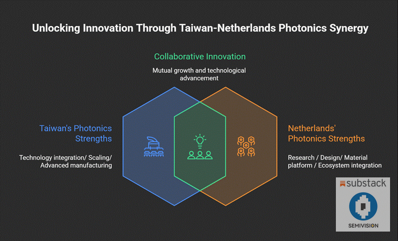
Taiwan and the Netherlands hold complementary strengths across the photonics value chain, and a future bilateral model should build on four pillars.
The first is production alignment and supply-chain integration. Europe excels in PIC design, materials, and prototype manufacturing, while Taiwan leads in high-volume wafer processing and advanced packaging. A coordinated model would connect European InP/SiN design houses with Taiwan’s large-scale foundries and OSATs, enabling European PICs to scale beyond pilot volumes. Joint ventures, long-term licensing, or shared IP frameworks could overcome confidentiality barriers. Governments could even co-fund a dedicated PIC packaging center in Taiwan to compensate for Europe’s limited back-end capacity, creating a unified cross-border supply pipeline.
The second pillar is cooperation on standards and interface specifications. With multiple materials, tools, and workflows still evolving, Taiwan and the Netherlands can jointly push standardization in OIF, IEEE, and IEC working groups. Industry associations such as HiSPA, TOSIA and PhotonDelta could synchronize roadmaps and align feedback loops. Harmonizing PDK structures across Si, SiN, and InP platforms would improve design portability, while integrating European photonics models into Taiwan’s EDA ecosystem would streamline development.
The third pillar is platform integration and co-innovation. Since future systems will combine several materials in one package, both sides can collaborate deeply on heterogeneous integration. European InP laser arrays could be bonded onto Taiwan’s silicon-photonics ICs, or Taiwanese MEMS expertise could be applied to tunable photonic components. Joint research programs between institutes such as TU/e and ITRI can accelerate hybrid architectures tailored for next-generation datacom, sensing, and space communications.
The final pillar is talent mobility. Stronger academic and industrial exchanges would help bridge cultural and technical gaps. Taiwan could participate more formally in European training schemes, while Dutch institutions could host Taiwanese researchers in photonics-focused programs. A joint photonics innovation center—connecting top universities and companies from both sides—would anchor long-term collaboration and cultivate the next generation of PIC engineers.
In essence, PIC Summit Europe 2025 highlighted an industry moving from experimentation to coordinated growth. Mature platforms like InP and SiN continue to expand, new materials such as TFLN and Al₂O₃ are accelerating, and advanced packaging is emerging as the final barrier to mass deployment. Taiwan and the Netherlands, each strong in different layers of the stack, now have a unique chance to build a shared photonics ecosystem where design, manufacturing, integration, and talent development reinforce one another. This partnership model can help turn photonic chips into a foundational technology for AI, communications, healthcare, automotive systems, and quantum computing—and position both regions as co-architects of the next era of photonics.
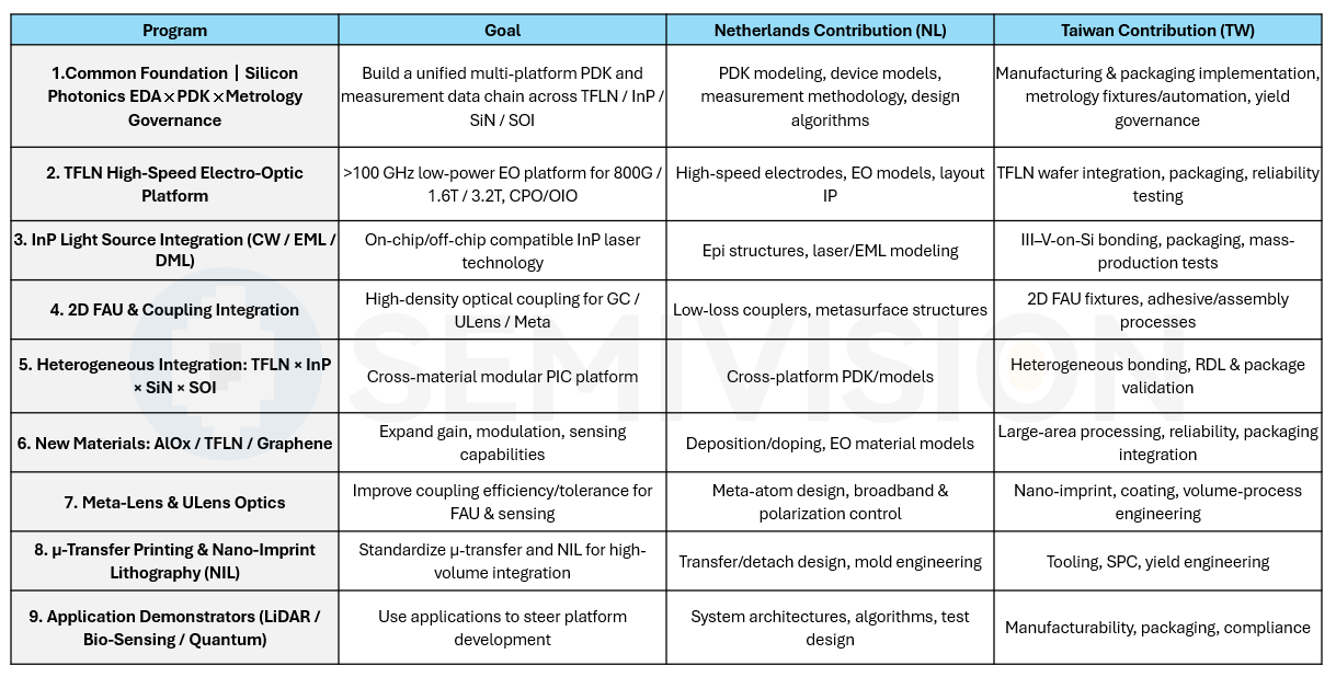
The nine topics below represent areas that SemiVision believes hold strong potential for collaborative development between the Netherlands and Taiwan following this PIC Summit Europe visit.
Taiwan has a powerful semiconductor industry. It ranks first in the world in foundry manufacturing and in packaging and testing, and currently second in IC design. In the past, Taiwan proudly promoted the phrase “Made in Taiwan.” Today, as the semiconductor industry evolves, Taiwan is shifting toward a new vision: “Made with Taiwan.” This concept emphasizes that true industrial strength must combine innovation, manufacturing capability, and co-creation. Taiwan is eager to share these strengths with global partners to advance the field of integrated photonics.
Historically and today, Taiwan is widely recognized for its silicon-based semiconductor leadership, with companies such as TSMC anchoring its reputation as a “Silicon Island.” Looking forward, Taiwan aims to evolve from a Silicon Island into a hub for photonic integration. Taiwan already possesses mature technical foundations that support this transition:
Wafer-to-package vertical integration, one of Taiwan’s strongest competitive advantages.
A robust semiconductor infrastructure spanning foundries, materials, tools, and OSATs.
The ability to extend these strengths from electronics into photonic integration, supported by both hybrid and heterogeneous integration approaches.
Taiwan’s photonic roadmap builds on combining different materials—SiN, SiO₂, InGaAsP/III-V, and emerging platforms—to create scalable, manufacturable photonic systems. Taiwan’s high-precision assembly, testing ecosystem, and “design-to-manufacturing” scalability provide a strong foundation for future global co-creation.
Evolution of Silicon Photonics and Future Needs
Silicon photonics is now a global focal point. Many companies worldwide are investing heavily in optical design, light sources, assembly, packaging, and testing. Taiwan hopes to serve as a bridge connecting experts in packaging, design, testing, and equipment, enabling cross-domain collaboration for next-generation photonic systems.
Strengthening Advanced Packaging Collaboration
Taiwan is home to global OSAT leaders such as ASE and SPIL, while Europe still lacks large-scale photonic packaging capacity. Dutch industry leaders repeatedly emphasized their desire to bring European-developed photonic chips to Taiwan for high-volume packaging. This would allow European companies to tap into Taiwan’s advanced lines, while giving Taiwan’s OSATs an early foothold in photonic products. Taiwanese delegates suggested forming a joint packaging task force to co-develop standards and solve challenges in CPO, fiber coupling, and thermal management. Albert Hasper, CEO of PHIX also noted that the gap between pilot production and mass manufacturing is an area where collaboration with Taiwan offers tremendous value. A future option is a EU-funded Taiwan -operated photonic packaging demonstration line to serve European customers.
Automated Testing and Standardization
Testing is another major bottleneck. Taiwan’s strength in precision machinery and automated test equipment can help introduce mature automation into the photonics domain. For example, Hsinchu firms have developed wafer-level optical alignment and measurement systems, and the STAr Technologies x CompoundTek collaboration already established silicon photonics wafer-level test solutions. Taiwanese delegates proposed that Taiwan and the Netherlands jointly drive international photonic testing standards—fiber-array probe interfaces, calibration procedures, reliability metrics—similar to SEMI standards in electronics. This would reduce fragmentation and enable the rise of third-party test service providers, improving efficiency and lowering costs. SEMI Taiwan can coordinate with PhotonDelta and JePPIX to form a global “Photonic Test Alliance.”
Cross-border MPW Collaboration
MPW services are essential for startups and academia. Europe has JePPIX (SiN/InP) and the US has AIM Photonics (SiPh). Taiwan’s SiPh MPW is emerging through TSRI and ITRI. Taiwan proposes a Taiwan–Netherlands MPW exchange framework, allowing Taiwanese teams to access InP/SiN MPWs and enabling European teams to prototype on Taiwan’s SiPh or TFLN lines. With a joint force, both Taiwan and the Netherlands could exchange MPW allocations, or co-host global MPW calls. This would accelerate innovation and resource sharing.
Talent Exchange and Knowledge Sharing
Ultimately, collaboration depends on people. Europe has deep photonics expertise but limited exposure to mass manufacturing, while Taiwan’s engineering talent excels at production but needs more photonics research immersion. A bilateral talent exchange—European postdocs working within Taiwan’s semiconductor companies, and Taiwanese engineers training in European photonics labs—would help bridge this divide. Workshops, summer schools, and a joint Taiwan–Netherlands Photonics Industry Forum could further strengthen constant knowledge flow. With HiSPA and TOSIA in Taiwan and PhotonDelta in Europe, aligning these organizations would help coordinate cross-border initiatives and information sharing.
Toward a Taiwan–Netherlands Photonics Axis
The delegation views this week’s PIC Summit as an excellent starting point. They invite all partners to attend the Taiwan Session—featuring a panel discussion and ecosystem networking—and to explore programs and success stories that can support deeper collaboration.
Taiwan’s strengths in high-volume manufacturing, packaging, and testing perfectly complement Europe’s leadership in photonic design, materials, and device innovation. To turn this synergy into global competitiveness, both sides must create long-term mechanisms across standards, talent, and manufacturing pipelines. With coordinated effort, a powerful Taiwan–Netherlands axis can emerge in the global photonics supply chain.
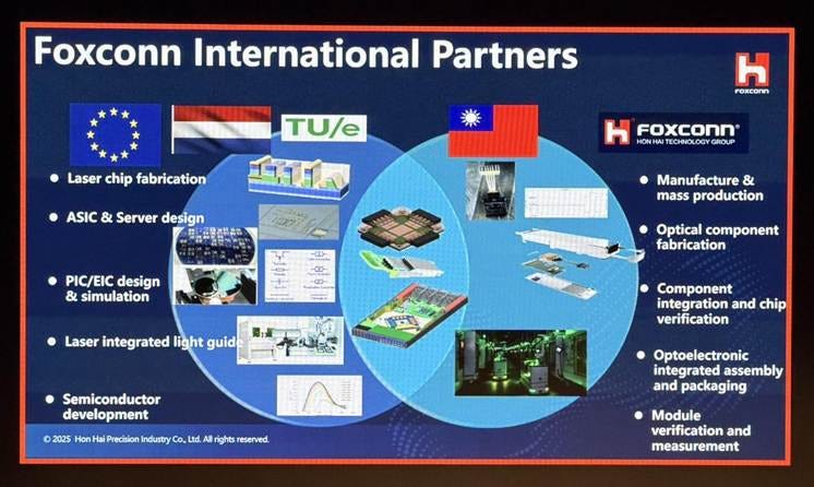
To conclude, Dr. Kuo’s slide from the Hon Hai Research Institute offers a clear illustration of how international collaboration can shape the future of integrated photonics. Europe and the Netherlands contribute foundational strengths such as laser chip fabrication, ASIC and server design, PIC/EIC simulation, and semiconductor development, while Taiwan provides the essential capabilities for scaling: advanced manufacturing, optical component fabrication, chip verification, optoelectronic assembly, and full-module testing. Together, these capabilities form a complete pipeline from innovation to mass production.
This slide also highlights an important message: the cooperation model between Taiwan and the Netherlands in integrated photonics can follow exactly this structure. It is an excellent example of how complementary ecosystems—Europe’s research and device innovation combined with Taiwan’s manufacturing and packaging expertise—can create a cohesive, end-to-end value chain. The next generation of integrated photonics, from high-speed optical interconnects to advanced sensing, will be enabled by this type of coordinated and scalable partnership.
Taiwan firmly believes it will be one of the Netherlands’ most important partners in the photonics era.
Dutch companies focus not only on technology development but also on application deployment and commercial validation. Several startups demonstrated how photonics enables high-performance sensing, data-center interconnects, LiDAR, and even medical diagnostics—highlighting a rapid transition from research to productization.
In Eindhoven, the Taiwan delegation visited TU/e (Eindhoven University of Technology), where faculty members hosted a comprehensive lab tour. The team gained firsthand insight into TU/e’s photonic R&D infrastructure, including waveguide fabrication, hybrid integration platforms, and new electro-optic materials such as TFLN and AlOx. These interactions highlighted the close coupling of fundamental science and engineering at TU/e, and the university’s role as a critical hub in Europe’s photonics research network.
At the end of the trip, the delegation traveled to Enschede, visiting key photonics companies and institutes including integrated photonics packaging specialist PHIX, and the materials and device research powerhouse MESA+ Lab. These visits demonstrated the strong synergy between Dutch academic research and industrialization, supported by government programs and venture ecosystems.
The Netherlands Photonics Landscape: A Full Value Chain from Research to Manufacturing

In recent years, the Twente–Nijmegen region has emerged as one of Europe’s most important hubs for integrated photonics and semiconductor technology. Anchored by the MESA+ nanotechnology center, ChipTech Twente, PHIX, and a growing wave of startups such as Brilliance, Aluvia Photonics, Chilas and SuperLight Photonics, the region now features a complete value chain spanning chip design, manufacturing, packaging, and system integration.
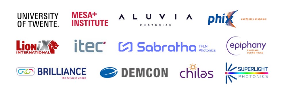
Aluvia Photonics: Spin-off from the University of Twente developing tunable lasers and high-speed modulators for PEC applications. Positioned as a photonics startup with strong electro-optic integration potential.
SuperLight Photonics: Builds high-brightness visible-light laser sources with strong energy efficiency. Targets AR/VR, wearables, and next-gen consumer photonics.
Chilas Lasers: Specializes in tunable and coherent lasers with ultra-stable single-frequency output. Serves coherent communications, LiDAR, and spectroscopy markets.
Sabratha Photonics: Focuses on Thin-Film Lithium Niobate (TFLN) platforms and high-speed EO modulators. Aims to bring TFLN devices into mainstream PIC manufacturing.
Epiphany Design: Provides design, prototyping, and system engineering for photonic components. Helps SMEs transition from concept to manufacturable products.
Demcon: Expert in high-precision equipment and automation for PIC packaging and testing. Offers alignment, assembly, and thermal-control solutions.
Itec Equipment: Supplies semiconductor and micro-assembly tools for PIC/MEMS packaging and testing. Supports high-speed bonding, laser welding, and automated inspection.
LioniX International: Leading Silicon Nitride (SiN) PIC platform provider with ultra-low-loss waveguides. Supports heterogeneous integration across InP/SiN/Si technologies.
Brilliance: Develops ultra-compact RGB laser chips designed for next-generation AR glasses and wearable displays. Their technology delivers bright, precisely controlled laser beams with low power consumption, enabling lightweight, all-day-wear AR devices.
Phix: a leading European packaging foundry for photonic integrated circuits, offering hybrid integration, optical assembly, fiber-array coupling, and scalable manufacturing across InP, SiPh, and SiN platforms. The company supports customers from prototyping to high-volume production, enabling reliable, industrial-grade PIC modules for global markets.
Throughout the multi-day program, the delegation visited numerous Dutch companies and research organizations, engaging in deep technical discussions and application-oriented exchanges. SemiVision observed that the Netherlands possesses a uniquely well-balanced photonic ecosystem: an upstream foundation in materials, wafer processing, and design tools; strong mid-stream competence in packaging and testing; and downstream strength in application integration. This creates a self-sustaining innovation engine.
From “Made in Taiwan” to “Made with Taiwan” — Co-Creating the Global Photonics Future
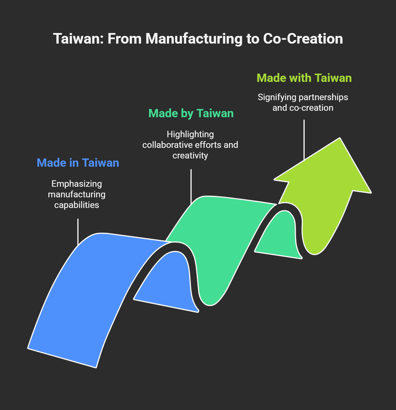
The Netherlands demonstrates Europe’s deep R&D strength and system-level innovation in photonics, while Taiwan provides unmatched capabilities in manufacturing, packaging, and supply-chain execution. Historically, collaboration followed the model of “EU design × Taiwan manufacturing.” Today, this is shifting toward a deeper framework: “Made with Taiwan.”
This new model positions Taiwan not only as a production partner but also as a co-innovator in materials, device development, heterogeneous integration, packaging and system deployment. Together, the Netherlands and Taiwan can form a “Cross-Border Innovation Chain” that spans design, wafer fabrication, advanced packaging, testing, and end-system applications.
This transformation is not merely supply-chain optimization—it is a new paradigm of co-development and shared value creation. As the photonics era accelerates across AI, communications, sensing, automotive and quantum technologies, Taiwan is positioned to become one of the Netherlands’ most important partners. Through the “Made with Taiwan” framework, both sides can jointly drive global photonics growth and shape the next decade of integrated photonics innovation.
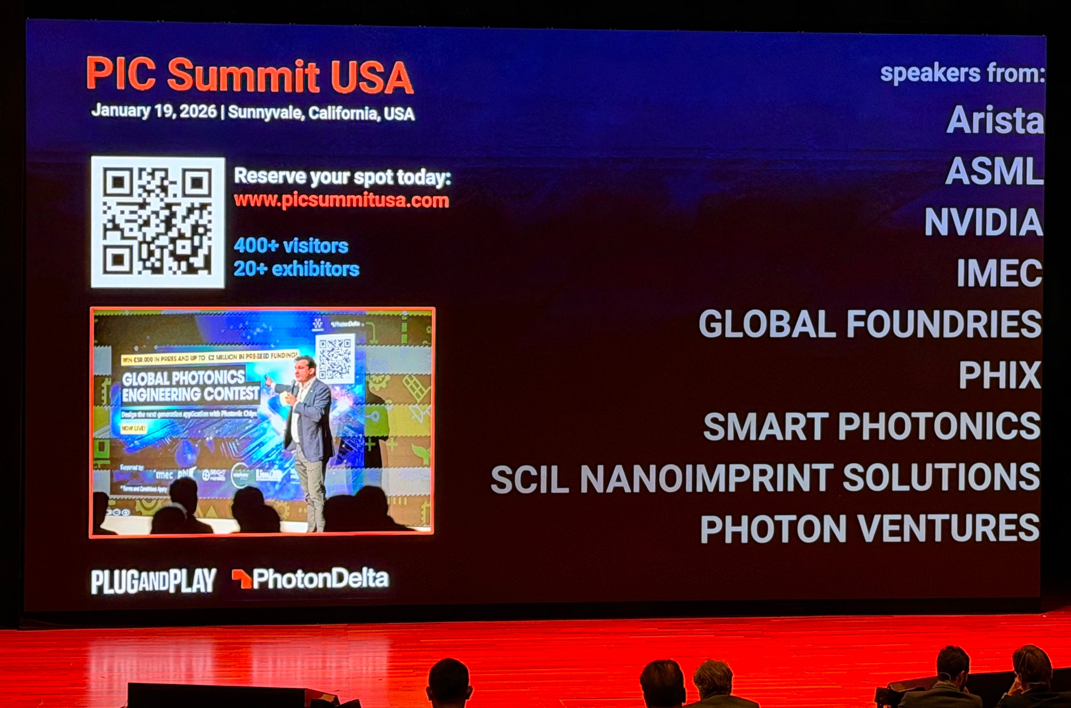
PIC Summit USA will take place on January 19, 2026 in Sunnyvale, California. The event will gather leading speakers from across the global photonics ecosystem, including NVIDIA, ASML, imec, GlobalFoundries, PHIX, Smart Photonics, and more.
If you’re interested in integrated photonics, this is an excellent opportunity to join.