Shaping the Future of AI Chips: Custom HBM and Advanced Packaging Lead the Way
From innovations in CoWoS and Hybrid Bonding to the shift towards 3D-IC and HBM integration, the race to redefine high-performance memory and computing intensifies.
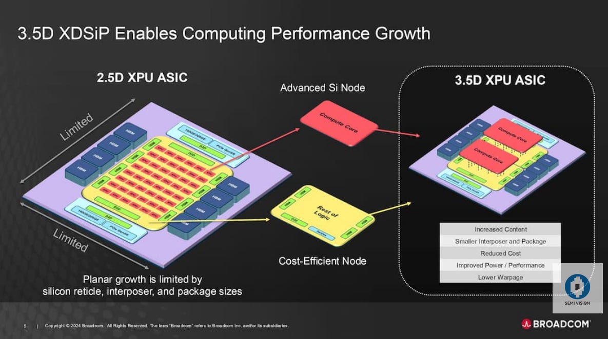
With the growing demand for advanced packaging, we have seen companies like Marvell and Broadcom launching their own advanced packaging platforms. For example:
Broadcom’s 3.5DXDSiP utilizes TSMC’s CoWoS-L packaging technology, enabling a packaging size approximately 5.5 times larger than the reticle size, with a total area of 4,719 mm². I…


