

The Infinite AI Compute Loop: HBM Big Three + TSMC × NVIDIA × OpenAI Shaping the Next-Generation Industry Chain
Original Article By SemiVision Research (TSMC, Nvidia, SKHynix, Samsung , Micron , CXMT , Marvell , Broadcom , AWS , GUC , OpenAI )

The development of AI has entered an unprecedented acceleration phase. From compute architectures and interconnect technologies to memory bottlenecks, the entire industry is rapidly revolving around a few key companies and technologies. NVIDIA’s recent wave of massive investments has popularized what many in the industry now call the “AI perpetual motion cycle.” In this cycle, AI chips drive compute demand; compute demand stimulates infrastructure investment; and infrastructure, in turn, fuels further expansion of AI chip applications.
However, at the foundation of this entire cycle lies TSMC’s advanced process and packaging capabilities.
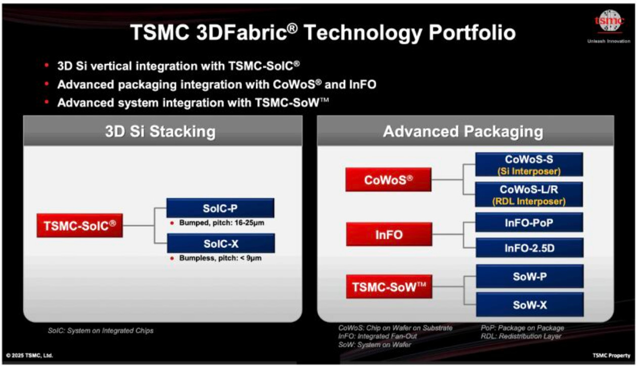
Today, AI chips and high-bandwidth interconnects have fully entered the “advanced process + advanced packaging” era. Whether it’s optical engines, sub-3 nm AI logic nodes, or various advanced packaging technologies such as InFO, CoWoS, SoW, and CoPoS, and even future SiC interposers (CoSoS), TSMC remains the sole strategic hub capable of supporting the entire stack — from design and manufacturing to packaging and system integration. At the same time, the industry has started using the term CoWoP, where the “P” refers to both PCB and the broader platform concept, emphasizing the depth and breadth of future system-level integration.
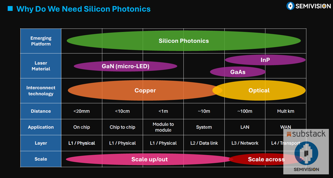
For an AI chip to truly achieve high performance, it’s not just about the process node. It involves ASIC design services, power and signal integrity (PI/SI), and high-speed transmission planning from RDL copper interconnects to optical engines, all of which drive fundamental changes in data center architecture. NVIDIA’s cluster strategy is evolving from Scale Up and Scale Out toward Scale Across, accelerating the adoption of Optical Circuit Switching (OCS). From PIC (Photonic Integrated Circuits) to MZI (Mach-Zehnder Interferometer) designs and next-generation transmission materials (e.g., TFLN, BTO, SOH) supporting speeds beyond 400 G, the entire high-speed optical interconnect ecosystem is being rapidly restructured.
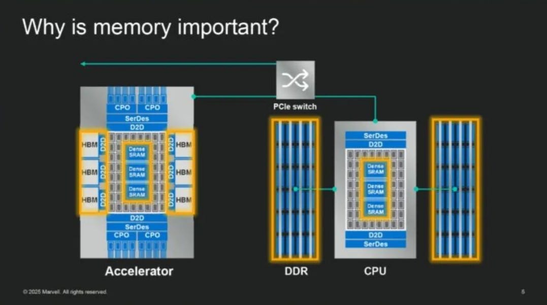
However, the ultimate performance boundary of AI systems is determined not only by compute and interconnect but also by memory. GPU performance has been advancing far faster than HBM (High Bandwidth Memory), creating a widening memory wall that has become a central industry focus in 2025. Marvell Technology has proposed concrete solutions for memory architectures and optical interconnects at HOT CHIPS 2025 and OCP Global Summit 2025, signaling a new wave of innovation to address this critical bottleneck.
The development of HBM goes far beyond memory process technology alone — it represents a deeply coupled engineering system with advanced packaging. From TSV (Through-Silicon Vias) and TCB/HCB/HB bonding to the gradual incorporation of the Base Die into TSMC’s process roadmap, HBM has become inseparable from leading-edge integration. This means that in the future AI race, the ability to master logic process + memory integration + optoelectronic packaging + interconnect architecture will be the decisive factor across the value chain. And at the center of all these critical nodes stands TSMC.
This article begins by examining the technological pillars behind the “AI perpetual motion machine”, focusing on the evolution of HBM processing technologies, the industry-wide challenge of the Memory Wall, and the strategic implications of optical interconnects and packaging platforms for future AI architectures.
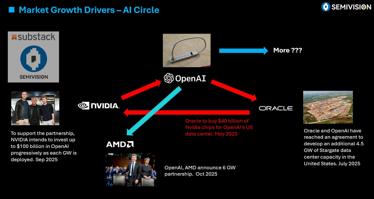
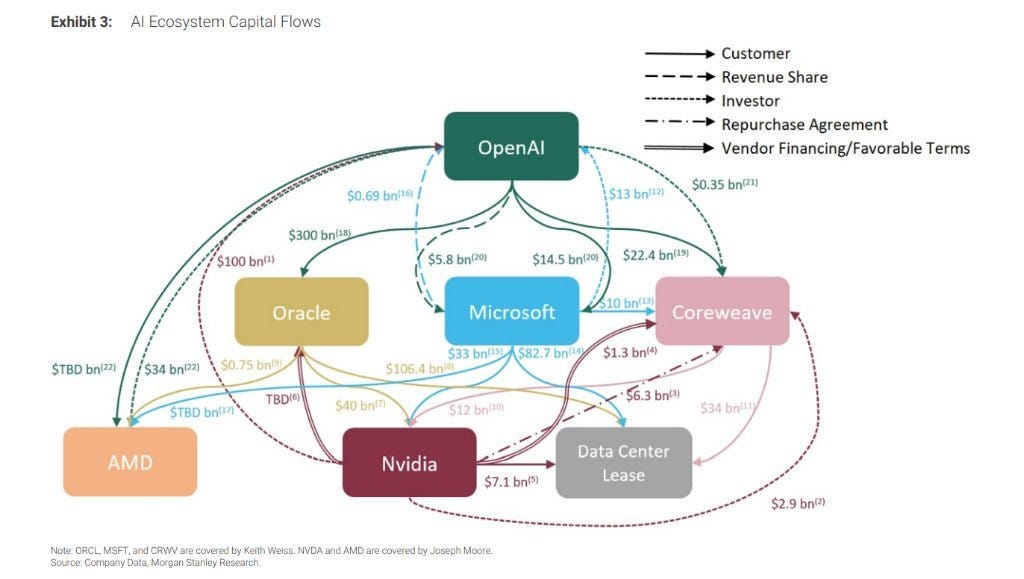
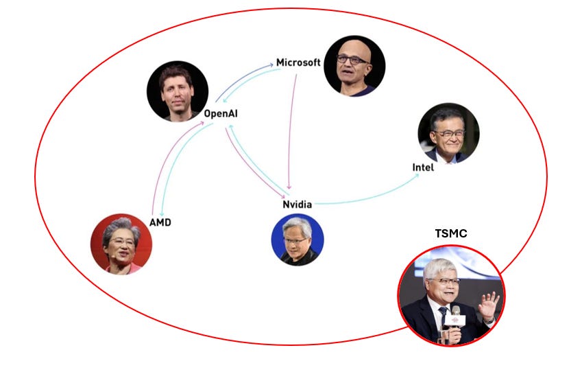
The vast interweaving of capital and technological ecosystems between NVIDIA and OpenAI — spanning hardware supply chains, cloud services, investment strategies, and startup networks — forms a powerful financial engine that drives the AI boom. Yet behind this flow of capital and compute lies a hidden strategic hub: TSMC.
From NVIDIA’s GPUs to AMD’s compute chips and large-scale cloud server processors, nearly all rely on TSMC’s advanced process nodes and 3DFabric packaging capabilities for production. In other words, behind every arrow in the capital–technology diagram, the true anchor of compute power is TSMC’s fabs and packaging platforms. Without TSMC, the ongoing AI capital explosion simply wouldn’t exist.
2026 Inflection Point: Systemic Reconstruction of AI Infrastructure
The year 2026 will mark a critical inflection point in the structural transformation of the AI industry. Over the past few years, performance gains in large models have been driven by parameter scaling and GPU cluster expansion. But as compute power transitions from Exa to Zetta scale, exponential growth is hitting physical and engineering limits. The true bottlenecks are no longer GPUs themselves, but memory bandwidth, packaging interconnects, thermal management, and power supply. Compute is the engine, but bandwidth and thermal management are the drivetrain; when the drivetrain can no longer scale linearly, the entire value chain is redefined.
Energy and Thermal Become Strategic
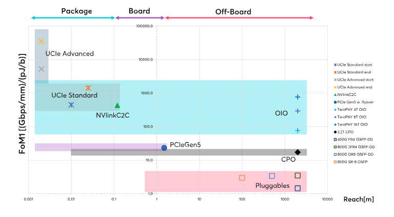
1 GW-class data centers are driving the adoption of liquid cooling and microfluidic (MCLP) technologies. High-thermal-conductivity diamond materials are emerging as mainstream heat spreaders. Site selection now depends on both grid capacity and water resources. Meanwhile, electrical interconnects are approaching physical limits in bandwidth and power efficiency, making CPO (Co-Packaged Optics) and OIO (Optical I/O) the core of the next architectural shift.
Industry Realignment: From NVIDIA-Centric to Distributed Control
Cloud service providers (CSPs) such as OpenAI, Google, Meta, AWS, and Huawei are pursuing “de-NVIDIA-ization” strategies—developing their own ASICs and purchasing HBM directly. This disperses pricing power and turns advanced packaging capacity into a strategic resource. HBM is no longer “just DRAM,” but a deeply integrated system of logic, memory, and interposers.
The technical focus is shifting from stack height to bandwidth engineering. Capabilities in RDL (Redistribution Layer) and PDN (Power Delivery Network) design are becoming key performance bottlenecks. In the short term, CoWoS-R supports scaling, while CoWoS-L and SoIC are expected to dominate mass production in the longer term.
Beyond Packaging: CXL and Photonics Reshape Memory Systems
The CXL (Compute Express Link) architecture is enabling resource pooling and near-memory compute. CXL 2.0/3.x combines Switching, Pooling, and P2P topologies, using OS-level hot page migration and remote memory scheduling to increase bandwidth utilization. However, maintaining high performance ultimately requires optical interconnect.
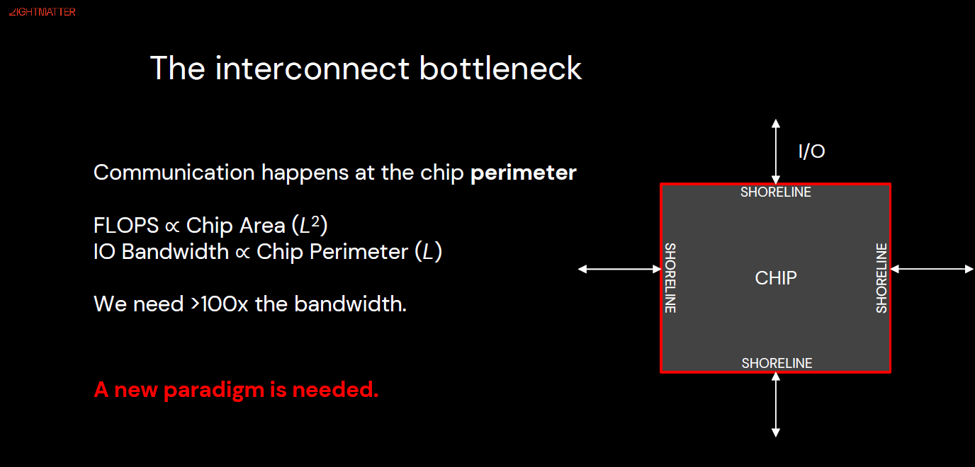
Companies like Ayar Labs, Celestial AI, Lightmatter, and Ranovus are breaking through packaging and reticle limits with silicon photonics, achieving nanosecond-level latency and Tb/s bandwidth, enabling distributed memory architectures. HBF/HFM technologies serve as the capacity layer, supplementing memory pools for large-scale inference at lower cost.
The Final Battleground: Packaging Space and System Design
The strategic competition ultimately returns to advanced packaging and system co-design. Asymmetric HBM placement, multi-layer RDL, PDN partitioning, and optical module integration are driving STCO (System-Technology Co-Optimization) to become the mainstream design methodology. Companies with strong packaging integration capabilities will command the new value chain.
Marvell and Broadcom are pushing custom HBM solutions and in-package optical interconnects to enter emerging markets.
TSMC is reinforcing its leadership through HBM base-die technology and CoWoS/SoIC platforms.
Korean–U.S. alliances dominate high-end HBM capacity, while China faces structural pressure.
2026: The Year of Repricing Bandwidth, Power, and Packaging
By 2026, electricity, water resources, advanced packaging capacity, and optical interconnect capability will all be repriced. The winners will be those who can convert bandwidth engineering into productivity and pricing leverage. This is not merely a technological race—it is a reorganization of power across the supply chain and infrastructure layers.
Risks on the Horizon and Challenges remain:
AI scaling laws may face diminishing returns.
CPO’s thermal management and maintainability issues are not yet fully solved.
CXL’s NUMA software overhead could slow commercialization.
HBF latency limits its usefulness in training scenarios.
As wires become antennas and photons replace copper, the future power structure of AI infrastructure will belong to those who can orchestrate bandwidth, thermal, and energy systems into a coherent whole.
For Paid Members , SemiVision will discuss topics on
The Breakpoint in AI Capability Curves: A Critical Nonlinear Leap by 2026
The Evolution of HBM, HBM IP, and the Memory Wall Challenge
The Concept of HBM IP
TSMC’s Strategic Position in the HBM Base Die Ecosystem
Bandwidth Limits and Packaging Bottlenecks: From DRAM Scaling to RDL Electrical Control
From CoWoS-R Validation to System-Level Packaging Integration
The Memory Wall Problem
Memory Allocation and Expansion under the CXL Architecture
Memory Expansion and Allocation
Solutions Combining Optical Chips and Memory
Celestial AI Photonic Fabric
Lightmatter Passage M1000
Ayar Labs TeraPHY Optical I/O
Ranovus (Odin) Multi-Wavelength Optical Platform
Academic Research: Optical Multi-Stacked HBM
Will HBM Be Replaced by Flash? — The Potential of HBF/HF
SemiVision’s Quick FAQ on HBM & Memory Technologies
Q1: How has HBM evolved across generations, and what are the key features?
Q2: What is HBM IP and why is it needed?
Q3: What is the “Memory Wall” and why does it exist?
Q4: How does CXL address memory allocation challenges?
Q5: How can optical chiplets and photonics help overcome the Memory Wall?
Q6: Will Flash replace HBM in the future?
Technology Advancement for Performance Boost in TSMC’s viewpoints
HBM Allocation and Packaging Space Optimization Strategies
Marvell : SRAM — Boosting Bandwidth and Efficiency in AI/XPU Devices
Marvell: Custom HBM — Tailoring Memory to Match XPU Requirements
Marvell’s Custom HBM Architecture
Marvell : CXL — Expanding and Sharing Memory Through Compute Express Link
Structera A: Near-Memory Accelerator
Integrated Perspective: Marvell’s Memory Strategy
Advantages and Limitations of ASICs in AI Inference
Why are major tech giants investing in custom ASICs?
ASIC WAR : The Race Toward Specialization and Systemization
The Impact of the AI Chip Era on Memory and HBM
Memory Requirements for AI Training and Inference
Large-Scale Clusters and CSP In-House ASIC Development
HBM: The Key Memory Technology Behind Generative AI
1. Basic Structure and Advantages of HBM
2.HBM Manufacturing and Competitive Landscape
3. HBM Supply-Demand Outlook and Market Size
Why Cloud Service Providers Develop Their Own AI ASICs
ASIC Growth Drives HBM Demand
HBM Competitive Landscape and Supply Chain Evolution
Cerebras :Near-memory computing and HBM alternatives
Summary of Explosive Growth of the HBM Market
Structural vs. Cyclical Cycles — Will AI Reshape the Traditional Memory Boom–Bust Pattern?
HBM4e and Advanced Logic Process Competitiveness — Process Dependence and Strategic Collaboration in Next-Gen Memory
Strategic Collaboration Models Between Foundries and Memory Vendors
Edge AI and Mobile HBM Technology – The Outlook for High-Bandwidth Memory in Smartphones, XR, and Automotive Devices
Breakthrough Conditions: Power, Packaging, and Cost
Strategic Implications for the Edge AI Era
Supply Chain Bottlenecks and Capacity Expansion — Key Factors in HBM / Advanced Memory Manufacturing
Materials and Process Equipment Bottlenecks in Memory Device
Strategies to overcome these bottlenecks
Materials and Process Innovations – Impact of New Technologies on Yield, Cost, and Capacity
5 nm Base Die and Logic Packaging Innovations:
Risk Management and Road-Mapping for New Process Technologies
