

The Next AI Packaging Bottleneck: Why TSMC Is Preparing for Glass and CoPoS
Original Article By SemiVision Research [Reading time: 15 mins]

The Next AI Packaging Bottleneck: Why TSMC Is Preparing for Glass and CoPoS
Glass is rapidly becoming one of the most discussed materials in advanced semiconductor packaging. Yet much of the market narrative remains oversimplified.
SemiVision found that some investors assume that TSMC’s CoPoS roadmap means the company is preparing to replace silicon interposers with glass. Others believe glass core substrates will immediately displace ABF substrates once panel-level packaging enters production. Neither interpretation fully reflects how TSMC is likely approaching the technology.
TSMC’s strategy is more gradual and more pragmatic.
The company is not making a single, all-in transition from silicon and organic materials to glass. Instead, it is building a multi-stage packaging roadmap in which different forms of glass solve different engineering problems at different times.
The first step is not necessarily a glass interposer. It is panelization.
CoPoS, or Chip-on-Panel-on-Substrate, moves advanced packaging from a circular wafer format toward a rectangular panel architecture. Glass initially serves primarily as a temporary carrier that enables large-area redistribution-layer processing. At a later stage, glass may move deeper into the package as a structural substrate. Only after the manufacturing ecosystem matures could glass become a practical interposer platform for the largest AI systems.
This distinction is critical.
CoPoS addresses the limits of wafer-based manufacturing. Glass core substrates address the mechanical and dimensional limits of organic substrates. Glass interposers address the electrical and routing limits of existing interposer architectures.
These are related technologies, but they are not the same technology.
AI Is Turning Packaging into a System-Level Bottleneck
The rapid expansion of artificial intelligence infrastructure is changing the physical dimensions of semiconductor packages.
AI accelerators are becoming larger. The number of HBM stacks surrounding each compute die is increasing. Chiplet architectures are adding more logic, memory, I/O and power-management components inside a single package. Meanwhile, the electrical distance between these components must remain extremely short to preserve bandwidth and energy efficiency.
As a result, advanced packaging is no longer simply a back-end manufacturing process. It has become a system-level platform responsible for signal integrity, power delivery, thermal management and mechanical stability.
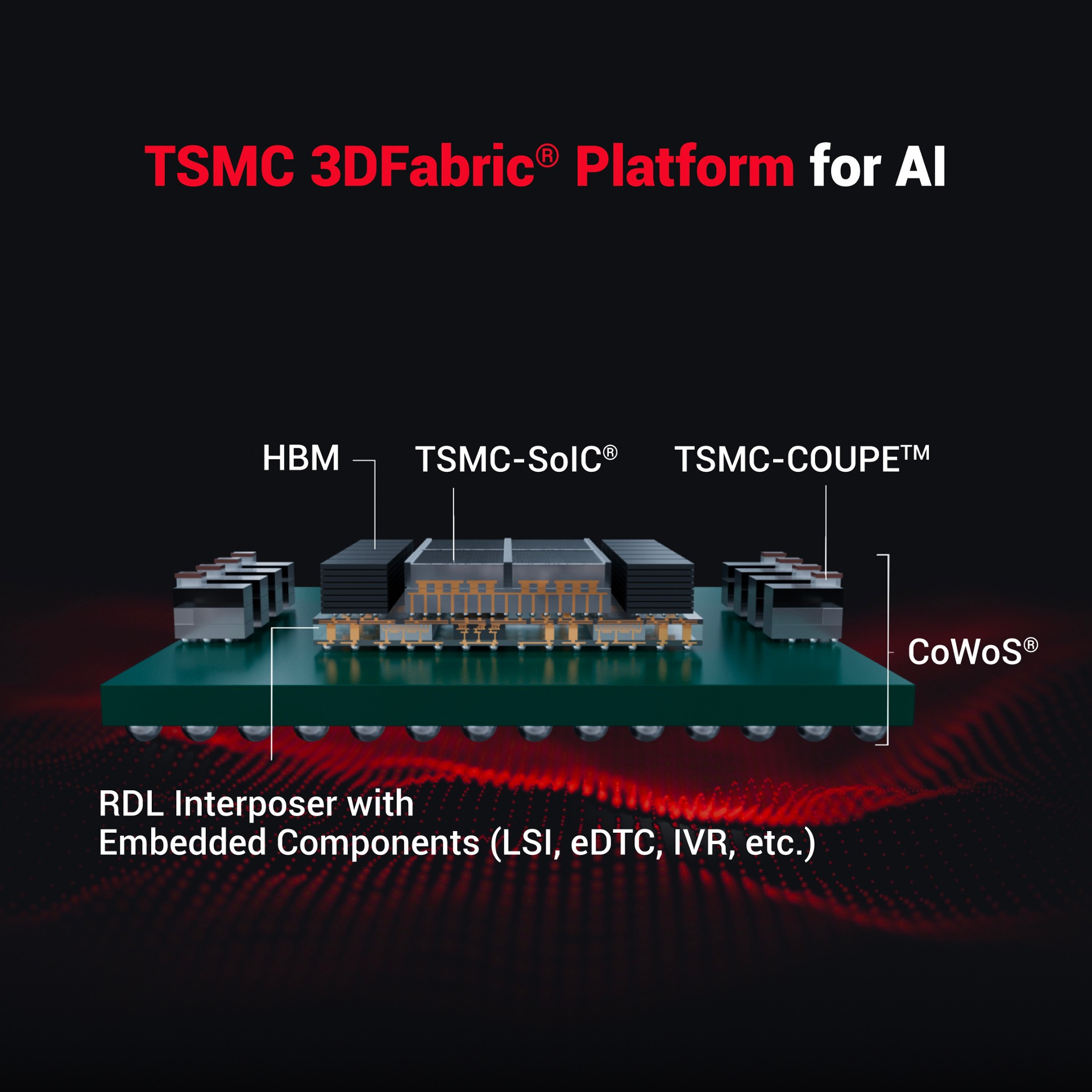
TSMC’s CoWoS platform has been central to this transformation.
CoWoS uses a wafer-based process to integrate GPUs, ASICs and HBM through silicon interposers or redistribution-layer structures. The platform is mature, highly integrated and supported by a broad manufacturing ecosystem. However, it is still constrained by the geometry of a circular wafer.
As AI packages become larger, fewer packages can be placed on each 300-millimeter wafer. The unused area around the edge increases, while each package consumes a larger share of the wafer. Adding more CoWoS capacity can alleviate shortages, but it cannot eliminate the fundamental geometric limitation.
This is why the next packaging transition is increasingly described as a move “from round to square.”
A rectangular panel can provide significantly higher area utilization than a circular wafer. It can also support larger package dimensions and potentially improve manufacturing economics once yields and process control become sufficiently mature.
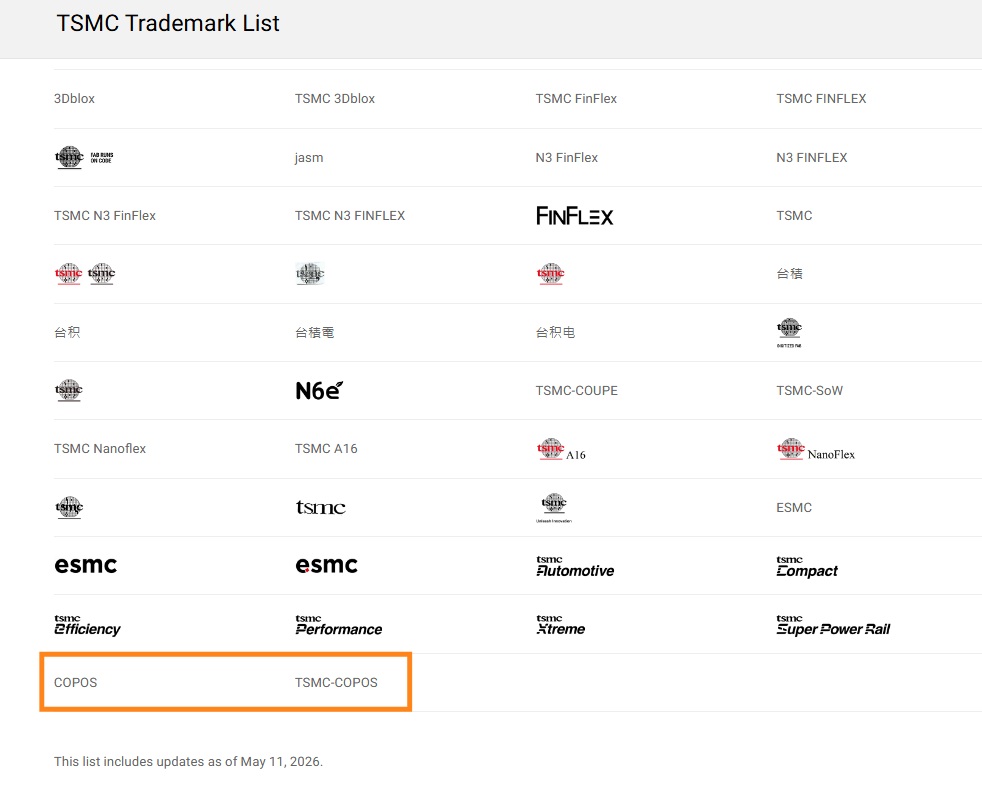
CoPoS is TSMC’s response to this scaling problem.
Below we will share:
CoPoS Is Primarily a Panelization Strategy
Glass Carrier, Glass Core and Glass Interposer Must Be Separated
Glass core Substrate Timeline
Intel Is Pursuing a Different Glass Strategy
Horizontal and Vertical Scaling Will Develop Together
Related report: SemiVision Technical insight Report – Glass, Advanced Package and TGV – Section 1
For more details and inquires please contact: jett@semivisiontw.com
