The Thermal Frontier of BSPDN: IITC 2025 Highlights from NYCU
Original Articles by SemiVision Research ( IEEE IITC , NYCU , TSMC )


This paper was presented at the 2025 IEEE International Interconnect Technology Conference (IITC) and is one of the most representative and significant studies this year on the thermal performance challenges of Backside Power Delivery Network (BSPDN) architecture. Led by Professor Kuan-Neng Chen of National Yang Ming Chiao Tung University, Taiwan, the research provides an in-depth exploration of the thermal conduction bottlenecks inherent to BSPDN systems. It employs a multi-level thermal simulation framework to thoroughly analyze the heat dissipation challenges spanning from the chip level to the package level.


At the 2025 IEEE ECTC, TSMC unveiled several advanced thermal management solutions aimed at addressing the challenges posed by high power density chips. These include innovations in thermal interface materials (TIMs), package-level microchannel cooling, and thermal simulation analysis of SoIC structures. Building on this, the paper presented by Professor Kuan-Neng Chen’s team at IITC further sharpens the focus by tackling system-level thermal resistance modeling and thermal diffusion path planning under the BSPDN (Backside Power Delivery Network) architecture, offering a highly engineering-relevant perspective.
Professor Kuan-Neng Chen currently serves as the Dean of the International College of Semiconductor Technology at National Yang Ming Chiao Tung University (NYCU) and holds the position of Chair Professor at the Institute of Electronics. He earned his Ph.D. in Electrical Engineering and Computer Science, as well as a Master’s degree in Materials Science, from the Massachusetts Institute of Technology (MIT). With over 20 years of experience in 3D integrated circuits (3D IC), heterogeneous integration, and advanced packaging, Professor Chen is widely recognized as a global leader in these fields.
Professor Chen has played a pivotal role across academia, industry, and policy. He was previously a researcher at IBM Thomas J. Watson Research Center, a visiting scientist at MIT, a visiting professor at IIT Bombay, and a distinguished professor at Tokyo Institute of Technology. He also served as Executive Director of the NSTC Microelectronics Program and as Deputy Director of the Industrial Technology Research Institute (ITRI). These diverse experiences enable him to lead talent cultivation and drive innovation across sectors.
Academically, Professor Chen has published over 400 journal and conference papers, contributed to 7 international book chapters, and holds 87 patents. He is a Fellow of multiple prestigious societies including IEEE, IET, IMAPS, and NAI, and has received several international honors such as the IEEE EPS Technical Recognition Award, IMAPS Technical Achievement Award, IBM Invention Achievement Award, and Taiwan’s National Industrial Innovation Award, attesting to his global influence in semiconductor and packaging research.
Professor Chen leads the 3DIC Lab at NYCU, which focuses on next-generation post-Moore system integration technologies. The lab’s research emphasizes 3D IC, advanced packaging, low-temperature heterogeneous bonding, and application-driven system design. Core research topics include:
Low-temperature copper bonding (e.g., ultra-thin barrier layers, Al/polymer hybrid bonding)
Monolithic 3D IC and bump-less wafer-level TSV
Hyper RDL interposer design
Biomedical and neuromorphic chip integration
MEMS packaging and heterogeneous SoC applications
The 3DIC Lab regularly contributes to top-tier international conferences such as IEDM, ISSCC, VLSI, and ECS, and collaborates with major global semiconductor companies and research institutes. Its research output not only has high academic impact but also advances industrial applications in heterogeneous integration and advanced packaging. The lab fosters a collaborative, open-discussion environment inspired by U.S. research culture and values interdisciplinary thinking and hands-on engineering. Students with a strong passion for semiconductors, materials, and system integration are highly encouraged to join.
The lab’s official website is: https://3dic.lab.nycu.edu.tw
The lab is located in Room ED521, Engineering Building IV at NYCU. Professor Chen’s office is in Room 506 of the same building. He can be reached via phone at +886-3-5712121 ext. 31558 or 54241, or via email at knchen@nycu.edu.tw.
In summary, Professor Kuan-Neng Chen is not only a leading figure in 3D IC and advanced packaging technologies but also a bridge between academia and industry. Under his leadership, the 3DIC Lab has become one of Taiwan’s most prominent research teams in post-Moore system innovation and heterogeneous integration, playing a critical role in the global semiconductor landscape.
Why is this paper significant?
1. Deep technical insight:
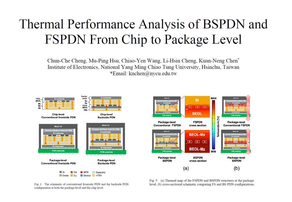
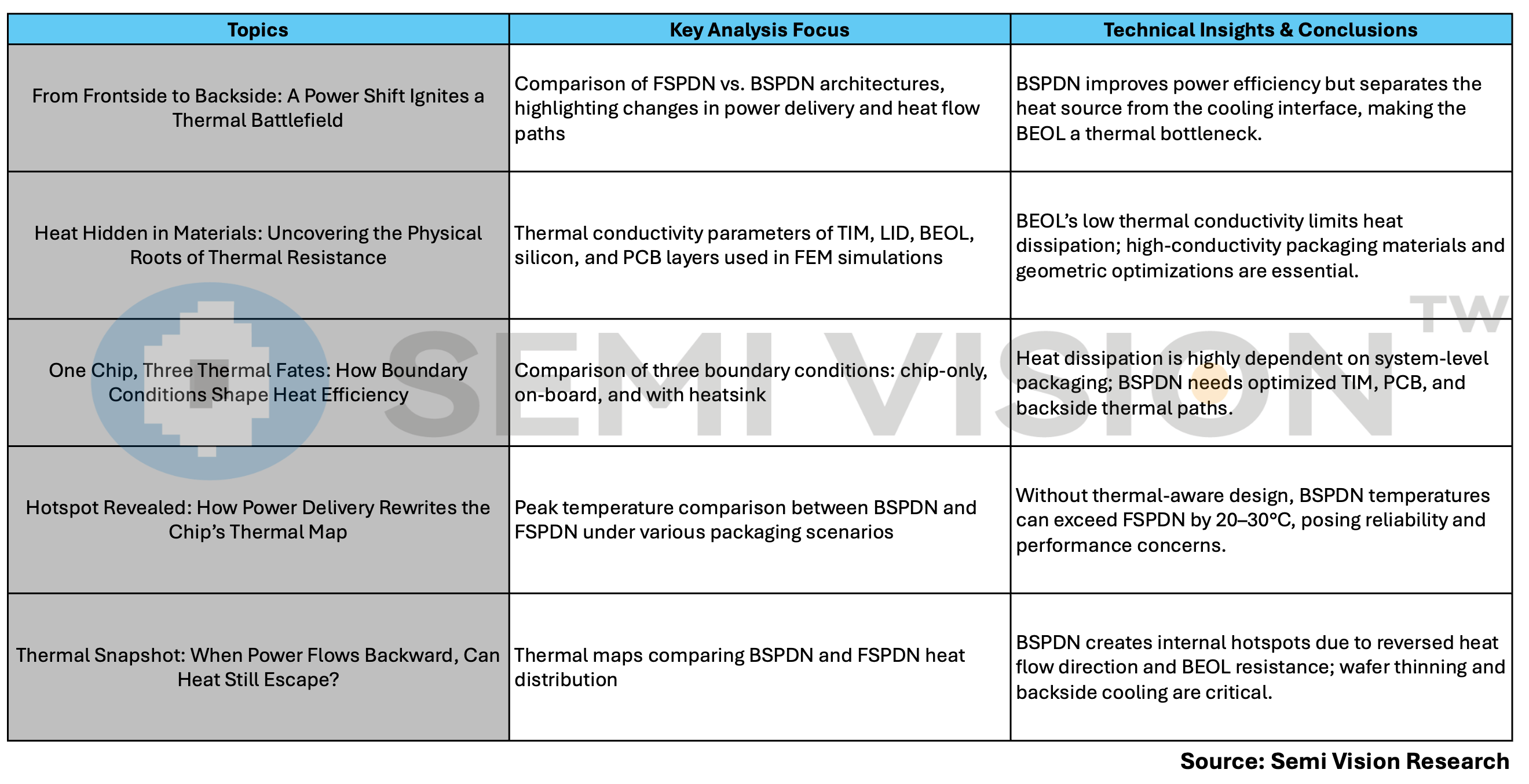
Unlike previous studies that approached BSPDN mainly from a conceptual or electrical optimization standpoint, this research concretely simulates the thermal resistance stack-up introduced by backside power delivery implementation. It highlights key challenges such as thermal bottlenecks in the BEOL, the reduced heat spreading efficiency after wafer thinning, and the vertical thermal resistance introduced by the integration of buried power rails (BPR) and nano-TSVs.
2. Cross-scale thermal analysis – from microscale to macroscale:
The study goes beyond chip-level microstructural thermal effects (e.g., in the BEOL and active layers) and extends into the package-level domain, examining thermal conduction behavior in elements such as interposers, underfill, and molding compounds. This results in a comprehensive chip-to-package thermal transfer model.
3. Identification of thermal “design bottlenecks”:
The results reveal that while BSPDN enhances power delivery efficiency and shortens current paths, it also shifts the main heat dissipation path from the frontside metal layers (used in traditional FSPDN) to the less favorable backside. This architectural change introduces thermal bottlenecks, making it more difficult to direct heat flow efficiently toward cooling components—posing a critical risk in the design of future high-power AI accelerators and HPC chips.
4. Bridging advanced process technology and system-level engineering:
The paper also emphasizes that addressing the thermal challenges of BSPDN requires holistic design efforts—spanning materials science, wafer-level process engineering, EDA tool development, and packaging integration. This underscores that thermal design has become an integral and inseparable part of next-generation chip development.

From IITC to ECTC, and from device-level to system-level, the power delivery advantages and thermal challenges of Backside Power Delivery Network (BSPDN) have emerged as one of the most critical topics in the evolution of advanced semiconductor processes. In this paper, Professor Kuan-Neng Chen provides the industry with a forward-looking and practically valuable technical reference, combining rigorous scientific modeling with a comprehensive system-level perspective.
SemiVision will provide an in-depth interpretation of this research under the topic.
For Paid Members ,SemiVision will discuss topics on
BSPDN vs. FSPDN: Thermal Performance Analysis from Chip to Package — Challenges and Breakthroughs
Intel – PowerVia
TSMC – Super Power Rail (SPR)
Samsung – SF2Z BSPDN
Deep Insights and Forward Outlook
Thermal Conduction Challenge: Balancing Power Efficiency and Heat Management
Simulation Results and Design Implications
A Thermal Design Mindset for Next-Generation Chip Architectures
Thermal Conductivity Parameters and Considerations in Heat Simulation
Comparative Illustration of Three Thermal Boundary Condition Configurations
Peak Temperature Comparison of BSPDN and FSPDN Under Varying Packaging Conditions
Thermal Distribution Comparison Between FSPDN and BSPDN Architecture