

TSMC and NVIDIA Pioneering the Future of AI with Silicon Photonics Technology
Addressing Key Technical Challenges and Advancements in PIC and EIC Integration, Optical Packaging, and TSMC’s High-Bandwidth Solutions.

NVIDIA showcased its AI GPU technology at the IEDM 2024 Global Semiconductor Leadership Conference in the United States, highlighting that, in the medium to long term, silicon photonics technology could significantly benefit chip-to-chip connections within AI data centers. This statement has garnered considerable attention within the semiconductor industry, emphasizing the potential of silicon photonics in driving advancements in AI technology.

Silicon Photonics (SiPh) is becoming essential due to the explosive growth of internet traffic and the increasing demands on data centers for higher speed and lower power consumption. Here's why SiPh is needed:
High-Speed Data Transmission: Traditional copper-based systems have limitations in terms of speed and reach. SiPh allows for high-speed optical communication that can support the growing data requirements, especially in data centers.

Source: TSMC Low Power Consumption: SiPh is more energy-efficient compared to traditional electrical interconnects, addressing the growing concern about energy usage in large-scale data centers.

Scalability: The Compact Universal Photonic Engine (COUPE) proposed by TSMC enables scalable solutions that cater to a wide range of applications in terms of performance, power, and cost.
Overcoming Distance Limitations: Optical technology significantly outperforms copper in terms of reach and bandwidth. SiPh is ideal for bridging the gap between short-reach interconnects (e.g., on-chip and on-board) and longer-reach applications (e.g., data center to data center).
Meeting Future Bandwidth Demands: As bandwidth needs double every two years, SiPh is crucial for keeping pace with this exponential growth, enabling technologies like 400G, 800G, 1.6T, and beyond.


Silicon Photonics (SiPh) is an advanced technology that integrates photonics (PIC) with CMOS electronic technology (EIC). Its core concept is to utilize silicon as a platform for optical signal transmission and processing, enabling high-speed and low-power optical communication and signal processing.
Silicon photonics is specifically designed for applications requiring high-speed transmission and high-bandwidth conditions. In the traditional optical module field, technologies like 400G and 800G currently do not employ silicon photonics. However, at the 1.6T level, the use of silicon photonics becomes necessary. Presently, manufacturers capable of producing PIC chips can be categorized geographically: in the United States, Intel and GlobalFoundries are leading, while in Taiwan, TSMC and UMC are the main players.

We have the clearest understanding of TSMC's silicon photonics roadmap. This diagram clearly illustrates that TSMC currently refers to its optical engine platform as COUPE (Compact Universal Photonic Engine). The primary purpose of this platform is to integrate PIC (Photonic Integrated Circuit) chips and EIC (Electronic Integrated Circuit) chips, produced by semiconductor foundries, through advanced packaging technologies such as hybrid bonding, stacking the PIC and EIC together to form an optical engine.

The applications for the optical engine are extensive. TSMC's current roadmap envisions its use in pluggable optical modules, with a bandwidth of 1.6 Tbps. This 1.6T optical engine (OE) is composed of both PIC and EIC components. Looking ahead, TSMC has also planned OE solutions with bandwidths of 6.4 Tbps and 12.8 Tbps.
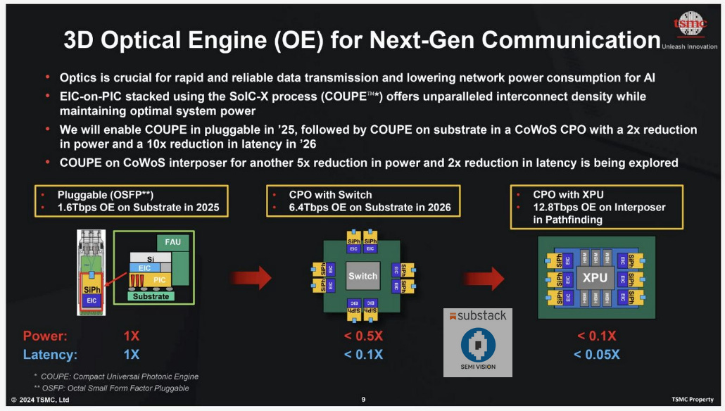
In the optical communications industry, bandwidth typically doubles every two years. For example, 400G upgrades to 800G, 800G to 1.6T, 1.6T to 3.2T, and finally 3.2T to 6.4T. Notably, TSMC has skipped the 3.2T OE design phase and plans to directly upgrade from 1.6T to 6.4T. The specifics of this upgrade can be discussed in more detail later.


We list the challenges faced in the development of silicon photonics:
PIC Chip Design (e.g., 1 split 4 channels or 1 split 8 channels)
Laser Intensity of CWDFB Light Sources
EIC Chip Design (e.g., CMOS, SiGe CMOS, advanced logic devices such as 7 nm)
Integration of PIC and EIC (Advanced packaging)
Microlens and Mirror Cavity Design
Coupling Technology (e.g., Grating Coupler or Edge Coupler)
FAU (Fiber Array Unit) Design
Measurement of PIC + EIC (Optical and electrical signals)
Challenges in Fiber Array
Stability and Reliability of Optical Adhesives

SemiVision define and shape customized technology studies, market research initiatives, and industry analyses. Our projects are tailored to address specific challenges, refine technology positioning, drive in-depth analysis, and deliver actionable, solution-oriented insights.
Contact us : jett@semivisiontw.com eddyt@semivisiontw.com