

TSMC and the Future of Semiconductors: Driving the AI-HPC Revolution
Original Articles by SemiVision Research (Dr. Kevin Zheng)

At the 2025 TSMC North America Technology Symposium, Dr. Kevin—drawing upon over 30 years of industry experience—delivered a comprehensive keynote that examined the semiconductor industry’s global landscape and its rapid transformation. Anchored in the rise of artificial intelligence (AI), big data, and high-performance computing (HPC), Dr. Kevin provided deep insights into how these disruptive forces are accelerating innovation across wafer manufacturing, technology development, and system architecture.
TSMC will be holding its forum in Taiwan on May 15, 2025, and SemiVision will continue to provide updates on TSMC’s latest technologies!
The following summary captures the key ideas and strategic perspectives outlined in Dr. Kevin’s presentation
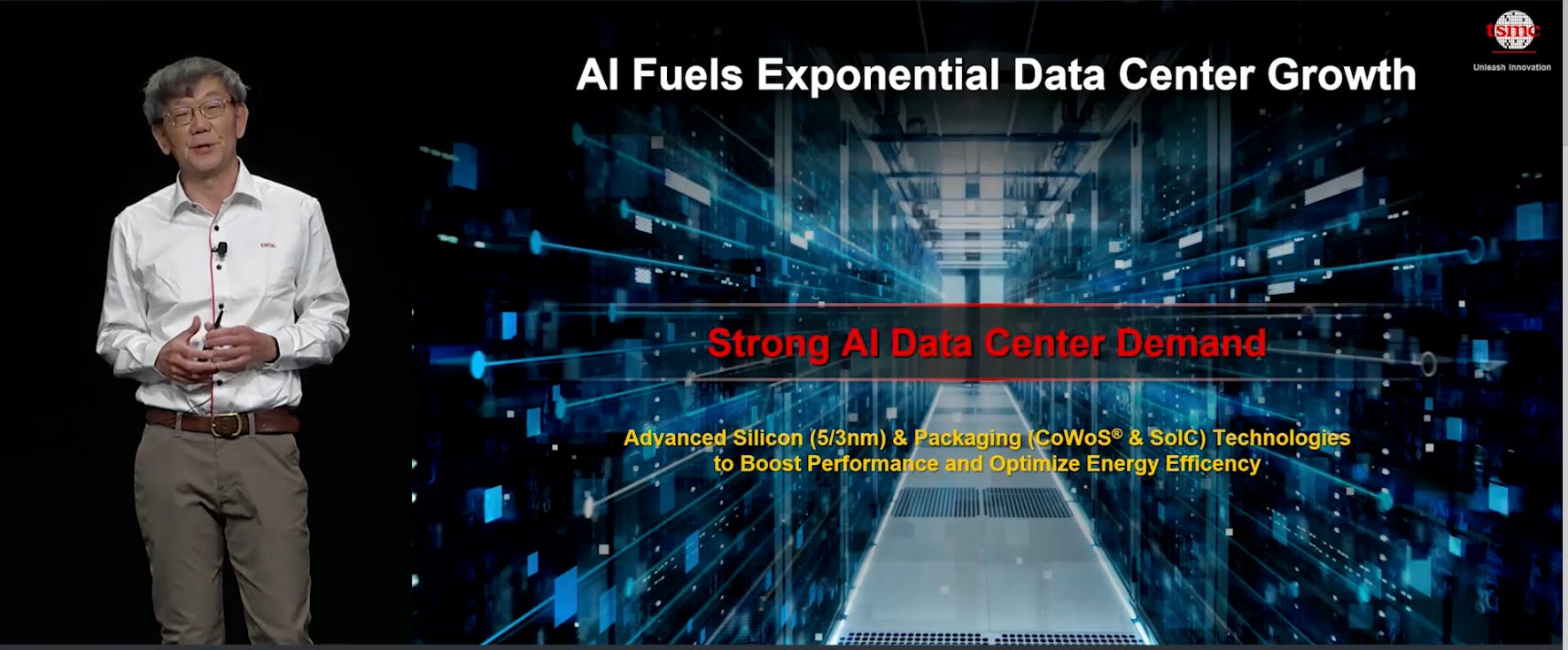
AI as the Catalyst for Explosive Data Center Growth
Dr. Kevin emphasized that artificial intelligence is no longer just a disruptive workload—it has become the primary growth engine for modern data infrastructure. The exponential increase in model complexity, parameter count, and training frequency has triggered an unprecedented surge in data center compute demands. This has led to massive investments in next-generation AI servers, GPUs, accelerators, and high-bandwidth interconnects. As a result, advanced semiconductor nodes are not only enabling more powerful AI chips, but also redefining system-level architecture to meet the scale, speed, and energy efficiency required for hyperscale AI workloads.
With the explosive rise of generative AI and large language model (LLM) workloads, the construction of AI data centers has entered an exponential growth phase. This wave of expansion is directly fueling unprecedented demand for advanced logic processes and high-performance packaging technologies, becoming a key force reshaping the global semiconductor industry landscape.
At the chip technology level, AI accelerators and server processors (XPUs) deployed in data centers increasingly rely on advanced 5nm and 3nm nodes to achieve higher compute density and energy efficiency. Meanwhile, as a single monolithic chip can no longer meet the surging demands for compute and bandwidth, heterogeneous integration has emerged as a necessary architectural approach to enable next-generation system scalability.

Among these advancements, TSMC’s CoWoS-L (Chip-on-Wafer-on-Substrate with Local Silicon Interconnect)technology has emerged as the standard packaging platform for next-generation AI accelerators and data center GPUs. CoWoS-L integrates several key innovations that enable ultra-high performance and scalability:
Large Silicon Interposer: Supports side-by-side integration of multiple high-bandwidth memory (HBM) stacks and compute dies (SoCs/XPUs), delivering ultra-high I/O density and low-latency interconnects.
Local Silicon Interconnect (LSI): Incorporates silicon bridge structures to further shorten critical paths and reduce signal transmission latency within the package.
Integrated Voltage Regulator (IVR) and Deep Trench Capacitor (DTC): Enhance power delivery stability and suppress voltage noise caused by high transient current loads.
Massive HBM3/4 Stacking: Enables extremely high data throughput, essential for generative AI training and large-scale model inference.
Together, these elements make CoWoS-L a foundational technology for the AI computing era, supporting the intensive bandwidth, power, and integration demands of modern data center workloads.
Taking NVIDIA’s latest Blackwell family chips (Blackwell B100/B200/B300 series) as an example, these AI processors are manufactured using TSMC’s CoWoS-L platform:
Each module integrates more than two large compute dies (fabricated on TSMC’s 4nm process) along with multiple stacks of high-bandwidth memory (HBM).
The total transistor count exceeds 200 billion, marking a new milestone in chip complexity.
The HBM memory bandwidth surpasses 3TB/s, enabling real-time training and inference of AI models with hundreds of billions of parameters per second.
CoWoS-L significantly improves overall energy efficiency of the AI system while reducing thermal and power delivery challenges.
Moreover, compared to conventional PCB or standard packaging approaches, CoWoS-L delivers order-of-magnitude improvements across multiple dimensions—power efficiency, interconnect bandwidth, and package footprint utilization. These advantages make it a critical enabling infrastructure for future deployments in hyperscale data centers, powering the next wave of generative AI and large-scale computing workloads.
For Paid Members, SemiVision will discuss topics on
Edge AI: Early-Stage Growth with Gradual Momentum
Global Semiconductor Market Outlook (2025–2030)
The Arrival of the Foundry 2.0 Era: Reshaping the Semiconductor Business Model
Expanded Role of Foundries: From Manufacturing to Full-Stack Integration
Continuous Energy Efficiency Gains: The Core Driver of Technological Advancement
From 2.5D to Heterogeneous 3D + Photonic Integration
Domain-Specific Technological Advancements(Smartphone/Automotive Electronics/Humanoid Robots/Internet of Things (IoT)/AR/VR/XR Devices)
TSMC Powers U.S. Semiconductor Innovation