


TSMC Strengthens Its Foundry Leadership with Latest Silicon Photonics Platform Advancements
Original Article by SemiVision Research (TSMC , Nvidia)

TSMC recently hosted a closed-door forum in Taipei focused on Silicon Photonics, featuring a keynote presentation by TSMC’s Vice President. The forum primarily addressed TSMC’s vision of Silicon Photonics as part of the “More than Moore” scaling roadmap. As this event was restricted to invited industry participants, SemiVision is referencing publicly available materials—such as IEEE conference papers—to share the key concepts and technology directions with a broader audience.
We have observed that TSMC actively participates in various prestigious academic and industry conferences, including OFC (Optical Fiber Communication Conference), VLSI Symposium, ETEC, and other IEEE-sponsored forums. While the total number of IEEE papers from TSMC on photonics remains relatively limited, TSMC’s patent portfolio in Silicon Photonics shows a strategic and well-structured deployment, covering device design, process integration, and packaging technologies.
Based on this, we believe TSMC is building a comprehensive ecosystem around Silicon Photonics, leveraging both academic contributions and industrial implementation. At SemiVision, we leverage insights from these forums and public materials to provide structured and accessible explanations of these developments for the broader industry community.
In the future, we will conduct a more in-depth analysis of the silicon photonics strategies and developments of Nvidia, AMD, Imec, TSMC, and SPIL.
TSMC’s Breakthrough: Launching the World’s First 200G MRM CPO Product — Ushering in the Silicon Photonics New Era
Building Blocks and Manufacturing Insights
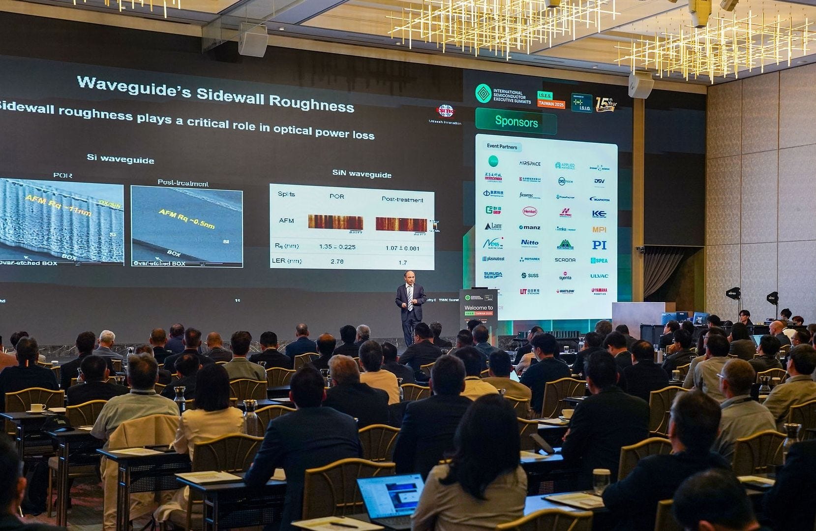
Attention to Waveguide Manufacturing Quality
2D Grating Couplers (2DGC) for Optical I/O
COUPE Platform and Silicon Photonics Integration
Technology Roadmap and TSMC Vision
Powering Tomorrow’s AI Infrastructure
Optical Testing – A Critical Challenge in Silicon Photonics