

TSMC x Nvidia : Breaking the Thermal Wall: How Advanced Cooling Is Powering the Future of Computing
Original Article by SemiVision Research (TSMC, NVIDIA, Coherent, Jentech, AVC, Auras, Cooler Master, Mikros Technologies, Inspur, Invek, Ningbo Jingda, Fabric8Labs, Intel , xMEMS)


The development of AI chips is fundamentally driven by the pursuit of higher performance, but this also brings a critical challenge: thermal management. Effectively dissipating the enormous heat generated by rising power consumption has become a key design consideration for next-generation AI chip architectures.
On the system level, the integration of optical engines is widely viewed as the future solution to overcome high-bandwidth interconnect bottlenecks. However, optical signals are highly sensitive to temperature fluctuations—even slight deviations can lead to transmission loss and degraded performance. This is why TSMC has adopted the Microring Modulator (MRM) approach, but MRM itself has strict thermal operating requirements. As a result, companies like TSMC and NVIDIA are actively exploring next-generation cooling technologies to meet these thermal demands.
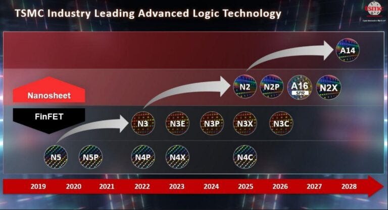
On the logic process side, TSMC’s evolution from N3 → N2 → A16 involves more than geometric scaling—it represents a transistor architecture transition: from FinFET, to GAA (Gate-All-Around), and finally to the Super Power Rail architecture in the A16 generation. This series of changes is aimed at achieving the optimal balance of PPA (Power, Performance, and Area), laying the foundation for high-efficiency AI computing.
However, from a packaging and materials perspective, new challenges emerge. Traditional cooling depends on TIM (Thermal Interface Materials), whose material selection is limited, and thermal reliability is constrained within specific temperature ranges. To address this, TSMC has proposed an innovative Direct Liquid Cooling (DLC) solution. By applying a backside copper pillar process, TSMC integrates microfluidic structures directly into the backside of the chip, allowing heat to be removed through direct liquid convection, dramatically increasing cooling efficiency.
Nevertheless, since no-TIM architectures are not yet fully mature, the industry currently relies on heat conduction through the top lid of the package for thermal management. This has led to the emergence of the Microchannel Lid (MCL) concept—micro-channels are etched directly into the internal surface of the package lid, combined with liquid cooling. MCL is expected to serve as a critical transitional solution before full backside liquid cooling becomes mainstream.
SemiVision believes that current AI chip logic process designs are almost exclusively carried out under high-density (HD) conditions. While this design approach significantly boosts computational performance per unit area, it also results in extremely high power density and heat flux, creating new thermal management bottlenecks.
A key question arises: Can the heat generated inside the AI chip be fully and evenly transferred to the package lid?
The internal thermal path of a chip involves multiple layers — silicon substrate, metal interconnects, micro-bumps, underfill, thermal interface materials (TIM), and more. Because of these layered thermal interfaces, heat cannot be transferred 100% efficiently to the lid, leading to localized “hotspots.” This cumulative thermal resistance is one of the primary factors limiting the chip’s maximum power output.
Improving Thermal Conduction Efficiency
The first key lies in shortening the thermal path and reducing interfacial thermal resistance at each layer, combined with introducing high thermal conductivity materials, such as:
Diamond thin films / CVD diamond
SiC substrates
Diamond Thin Film / CVD Diamond
Cu–diamond composites
These materials can dramatically increase the overall heat transfer coefficient.
Expanding Effective Heat Dissipation Area
The second key is increasing the effective surface area for heat exchange — enhancing convective heat transfer through larger fluid–solid contact areas. This has led the industry to explore several promising solutions:
(1) Microchannel Cold Plate (MCLP)
Approach: Etching micron-scale channels into copper or silicon substrates, with coolant flowing directly near the chip.
Advantages: Maximizes surface-to-volume ratio; significantly lowers thermal resistance.
Challenges: High pressure drop, clogging risk, and increased pump power consumption.
(2) SiC Substrate as Heat Sink
Material: Silicon carbide (SiC) has a high thermal conductivity of ~370–490 W/m·K, excellent mechanical strength, and high voltage tolerance.
Application: As a heat-spreading base substrate, it improves both thermal diffusion and mechanical/electrical performance, making it suitable for future >1 kW/cm² AI chips.
(3) Diamond Thin Film / CVD Diamond
Thermal Conductivity: 1000–2200 W/m·K — far surpassing silicon (~150 W/m·K) and SiC.
Application: Used as a heat-spreading interlayer or coating, directly deposited on chip or package surfaces.
Advantages: Ultra-low thermal resistance, nearly instantaneous hotspot dispersion; ideal for >500 W/cm² heat flux scenarios.
Challenges: High cost, complex CVD processes, and thermal expansion (CTE) mismatch with copper or SiC.
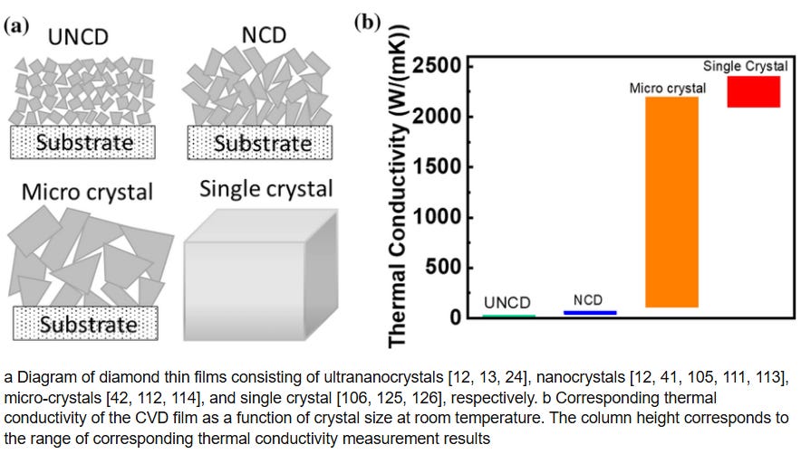
UNCD (Ultrananocrystalline Diamond) – composed of extremely fine grains on the nanometer scale.
NCD (Nanocrystalline Diamond) – slightly larger grain size than UNCD but still nanometer-scale.
Microcrystalline Diamond – composed of much larger grains, typically in the micron range.
Single-Crystal Diamond – a monolithic, defect-free structure without grain boundaries.
UNCD and NCD exhibit very low thermal conductivity, close to that of conventional semiconductors, due to extensive grain boundary scattering of phonons.
Microcrystalline diamond shows a dramatic increase, reaching values in the 2000–2200 W/m·K range, as larger crystal sizes reduce boundary scattering and improve phonon transport.
Single-crystal diamond exhibits the highest thermal conductivity, approaching 2500 W/m·K, making it one of the most thermally conductive materials known.
This clear correlation between crystal size and thermal performance is critical for selecting diamond materials for high-power electronic cooling. Microcrystalline and single-crystal diamonds are particularly promising for next-generation AI/HPC chip heat spreaders.
(4)Cu–diamond composites
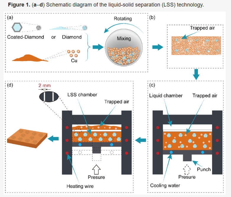
Diamond/Cu composite thermal management approach demonstrates outstanding potential for next-generation high-power electronic cooling. By incorporating Ti-coated diamond particles into a copper matrix using liquid–solid separation technology, the composite achieves exceptionally high thermal conductivity while maintaining strong interfacial bonding. The formation of a thin TiC interfacial layer plays a crucial role, significantly reducing interfacial thermal resistance and enabling efficient heat transfer between the diamond particles and the Cu matrix. With a measured TC of 457 W/m·K, and a theoretical potential exceeding 600 W/m·K at optimized coating thickness, this method offers a lightweight, mechanically robust, and thermally superior alternative to conventional heat spreaders. Its tunable structure through precise control of coating thickness and volume fraction makes it highly adaptable for AI/HPC chips, power devices, and advanced packaging platforms, where efficient heat dissipation is critical for stable, high-density operation.
TSMC and NVIDIA: Divergent but Complementary Strategies
TSMC focuses on evolving TIM, silicon-integrated microfluidics, and introducing SiC/diamond substrates, pushing the boundaries of materials and advanced packaging.
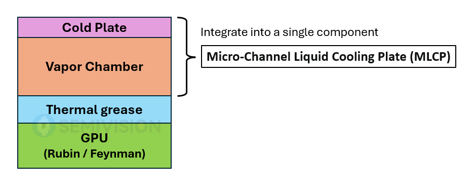
NVIDIA emphasizes MLCP, system-level liquid cooling (Direct-to-Chip and Direct-to-Silicon), and co-designing thermal and packaging architectures.
The Ultimate Goal
Both companies are converging on the same objectives:
Reduce thermal resistance
Increase effective heat dissipation area
Enable stable operation of future AI chips at higher power levels and higher densities
This thermal management evolution is becoming as critical as logic scaling itself in the AI computing era.
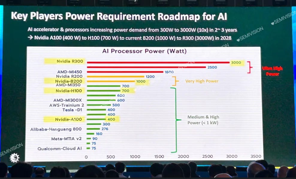
With the explosive growth of generative AI and high-performance computing (HPC), both chip power consumption and heat flux density are rising sharply. The thermal design power (TDP) of a single GPU or AI accelerator has already surpassed the kilowatt level, and is advancing toward the 3,000–5,000 W range.
While traditional air cooling and cold plate liquid cooling can delay thermal runaway, they struggle to cope with heat flux densities reaching as high as 800–1,000 W/cm². Against this backdrop, microchannel liquid cooling has become a new industry focus. By using micron-scale channel structures, it dramatically increases heat transfer surface area and fluid disturbance, achieving an unprecedented level of cooling efficiency.
For NVIDIA, sustaining energy-efficiency leadership in the next generation of AI GPU clusters means that thermal management has become just as critical a bottleneck as architecture design. As NVIDIA’s primary partner in advanced process technology and advanced packaging, TSMC is actively introducing microchannel liquid cooling into its 3DFabric platform (CoWoS, SoIC, etc.), exploring the possibilities of “in-package direct liquid cooling” and “chip-level direct cooling.”
This not only reflects TSMC’s view of cooling as a core component of Design-Technology Co-Optimization (DTCO/STCO), but also signals a paradigm shift in which thermal solutions will move from the system level down into the chip and packaging level, tightly integrated with process, packaging, and interconnect technologies.
As a result, the collaboration between TSMC and NVIDIA goes beyond process and compute—it is also evolving into a strategic alliance on thermal technology. With their joint push, microchannel cooling could become a defining inflection point in the AI chip era—reshaping the foundations of data center cooling infrastructure and potentially determining who can maintain leadership in the AI compute race.
As AI chip power consumption surges beyond 2,000 W and approaches 5,000 W, traditional air cooling and cold-plate solutions are no longer sufficient. How to efficiently dissipate multi-kilowatt heat flux within limited space is rapidly becoming the defining factor that separates leaders from followers in next-generation HPC and AI infrastructure.
In this premium feature report, SemiVision provides a comprehensive deep dive into:
Material Evolution
From traditional silicon substrates to SiC (Silicon Carbide), CVD diamond films, and Cu–Diamond composite materials—we analyze thermal conductivity advantages, integration challenges, and package-level compatibility.
The Four Stages of TIM (Thermal Interface Material) Evolution
From thermal grease → phase-change materials → metal solder → nanoscale direct bonding, we explore how the industry is progressively approaching the goal of “zero-interface” thermal resistance.
Breakthroughs in Microfluidic Cooling Technologies
MCL (Micro-Channel Lid) and MLCP (Micro-Channel Liquid Cooling Plate): technical paths, yield bottlenecks, and package-level reliability verification.
Two-phase flow and Critical Heat Flux (CHF) management, with optimized pressure-drop designs for large-scale integration.
Comparative analysis of laser machining, nano-etching, and 3D printing processes applied to copper, silicon, and SiC substrates.
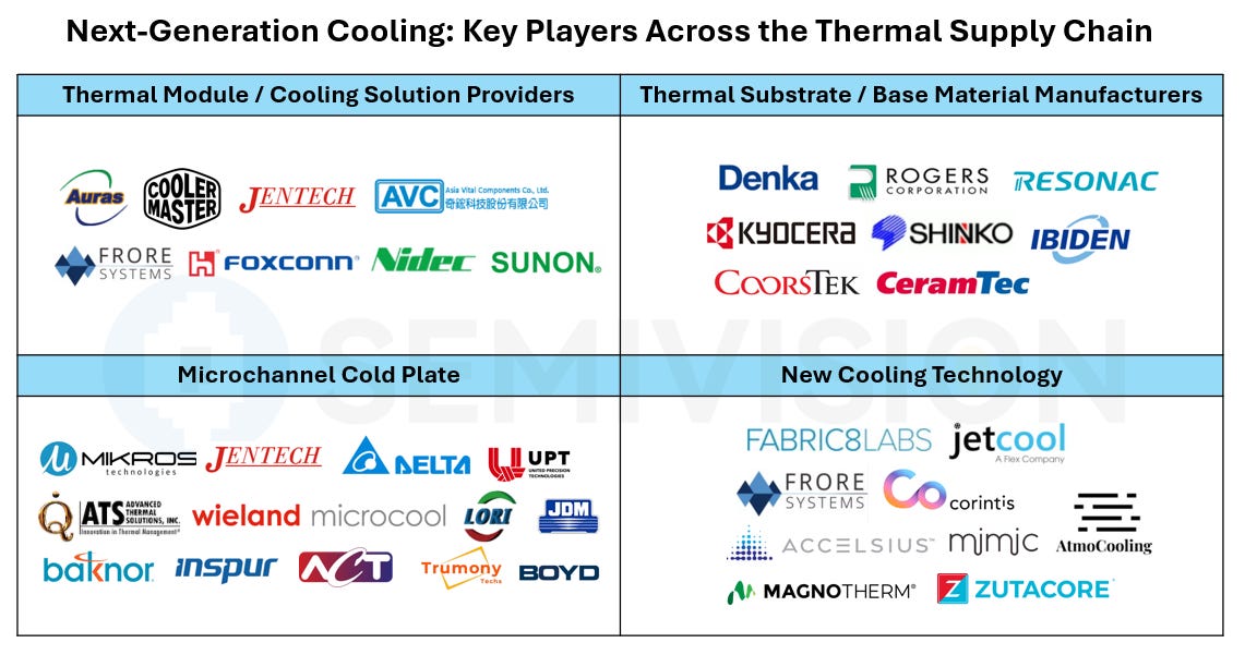
Supply Chain Landscape
From Taiwan’s four major thermal solution providers (Jentech, AVC, Auras, and Cooler Master) to China’s Inspur/Invek and Ningbo Jingda, and emerging innovators such as Fabric8Labs (ECAM technology) and xMEMS (µCooling active micro-cooling)—we assess who might take the lead in capturing this $5 billion next-generation cooling market.
Industry Trends
Why the NVIDIA Rubin generation is driving MLCP to become the new standard, and how TSMC’s 3DFabric platform is integrating direct liquid cooling, opening a new era of DTCO/STCO convergence across thermal management, packaging, power delivery, and optical interconnects.
These in-depth analyses reveal that AI thermal management is not merely an engineering challenge—but the new battlefield defining competitiveness across the semiconductor industry.
For Paid Members ,SemiVision will discuss topics on
Evolution of TIM Materials
SiC Substrates as a Future Concept for Microchannel Cooling
Thermal Management Technologies: Development and Future Trends
Vapor Chamber Lid (VC Lid)
Micro-Channel Lid (MCL)
More Advanced: Silicon-Integrated Micro-Coolers
System-Level Thermal Technologies in thermal management
Manufacturing Technology and Barriers
Core Concept of MLCP (Micro-Channel Liquid Cooling Plate)
Current MLCP Technology Progress and Challenges ( AVC & Auras & Cooler Master & JENTECH )
Why Microchannels Enable Much Higher Heat Flux Density per Unit Area
The Impact of Pressure Drop and Flow Distribution Inside Microchannels on Overall Cooling Performance
Heat Flux Density Supported by Microchannel Cooling in AI/HPC Chip Applications
Common Microchannel Fabrication Techniques: Advantages and Disadvantages
Machining Challenges for Different Materials (Silicon, Copper, SiC, Ceramics)
Methods to Ensure Geometric Accuracy and Surface Roughness of Microchannels During Fabrication
Addressing Interface Material and Reliability Issues in Direct-to-Chip Bonding of Microchannels
Will Microchannel Cooling Replace Traditional Cold Plates and Vapor Chambers as the Mainstream AI Chip Thermal Solution?
Microfluidic Cooling vs. Refrigerant-Based Direct Liquid Cooling — Which Is More Likely to Scale Commercially?
Will Microchannels Be Combined with Silicon Photonics (SiPh) or Co-Packaged Optics (CPO/OIO) to Provide an Integrated Thermal–Optical Platform?
Innovations Required for Microchannels to Handle 5000 W+ AI Chips (e.g., PCM Integration, Two-Phase Flow Control, Smart Monitoring)
Technological Breakthroughs and Industrialization Challenges of Microchannel Liquid Cold Plates (MLCP) in the AI Era
Demand Driven by NVIDIA: From Rubin to Rubin Ultra
Performance Leap: From Classical Models to Breakthrough Structures
Market Scale and Penetration: Liquid Cooling Becoming Mainstream
Supply Chain Landscape: From Thermal Vendors to System Integrators
Manufacturing Breakthroughs: Metal 3D Printing and Precision Sealing
Investment Opportunities and Key Components: From UQD to 3D Printing
From Technical Savior to Industry Standard
Fabric8Labs Shines at HOT CHIPS 2025
Why ECAM is Particularly Suitable for AI Thermal Management
Fabric8Labs:“ECAM Enabled Thermal Solutions for the AI Data Center”
Microchannel Cooling Innovation: From Machining to ECAM
Another cooling solution… xMEMS?
xMEMS µCooling / Fan-on-a-Chip Thermal Solutions