

TSMC’s SoW Renaissance: Defending the AI Frontier Where NVIDIA Sells Ecosystem, Not Chips
Original Article by SemiVision Research (IEEE ECTC ,TSMC , Nvidia , Tesla Dojo , Cerebras )

Why TSMC Doubles Down on SoW: Redefining AI System Integration in the Post-Reticle Era

As NVIDIA rises as the central force in AI infrastructure—selling not just chips, but complete compute systems—TSMC’s renewed focus on System-on-Wafer (SoW) reveals its strategic intent: to become the foundational enabler of next-generation AI superchips, where logic, memory, photonics, and power management are co-designed and co-packaged at wafer scale.
SoW is not just a packaging innovation—it’s a platform transformation, mirroring NVIDIA’s full-stack philosophy, and positioning TSMC as the shield behind the sword of AI computing.
At the 2025 IEEE ECTC, TSMC presented a wide range of papers focusing on AI chip design and advanced packaging architectures, covering innovations in CoWoS, System-on-Wafer (SoW), and emerging challenges such as thermal budget management. In this article, we focus specifically on TSMC’s SoW technology, which has attracted considerable attention.
The reason for this focus is that SoW technology originates from TSMC’s earlier InFO-SoW platform, for which several foundational papers are already available in IEEE literature. Therefore, we will not go into the legacy InFO-SoW in detail here. Instead, our discussion centers on how TSMC has redefined SoW in its latest architecture.
SemiVision: Some of these updates were previewed at the recent TSMC Technology Forum, but the most comprehensive technical details are found in the new paper presented at ECTC 2025, which forms the basis of our analysis.

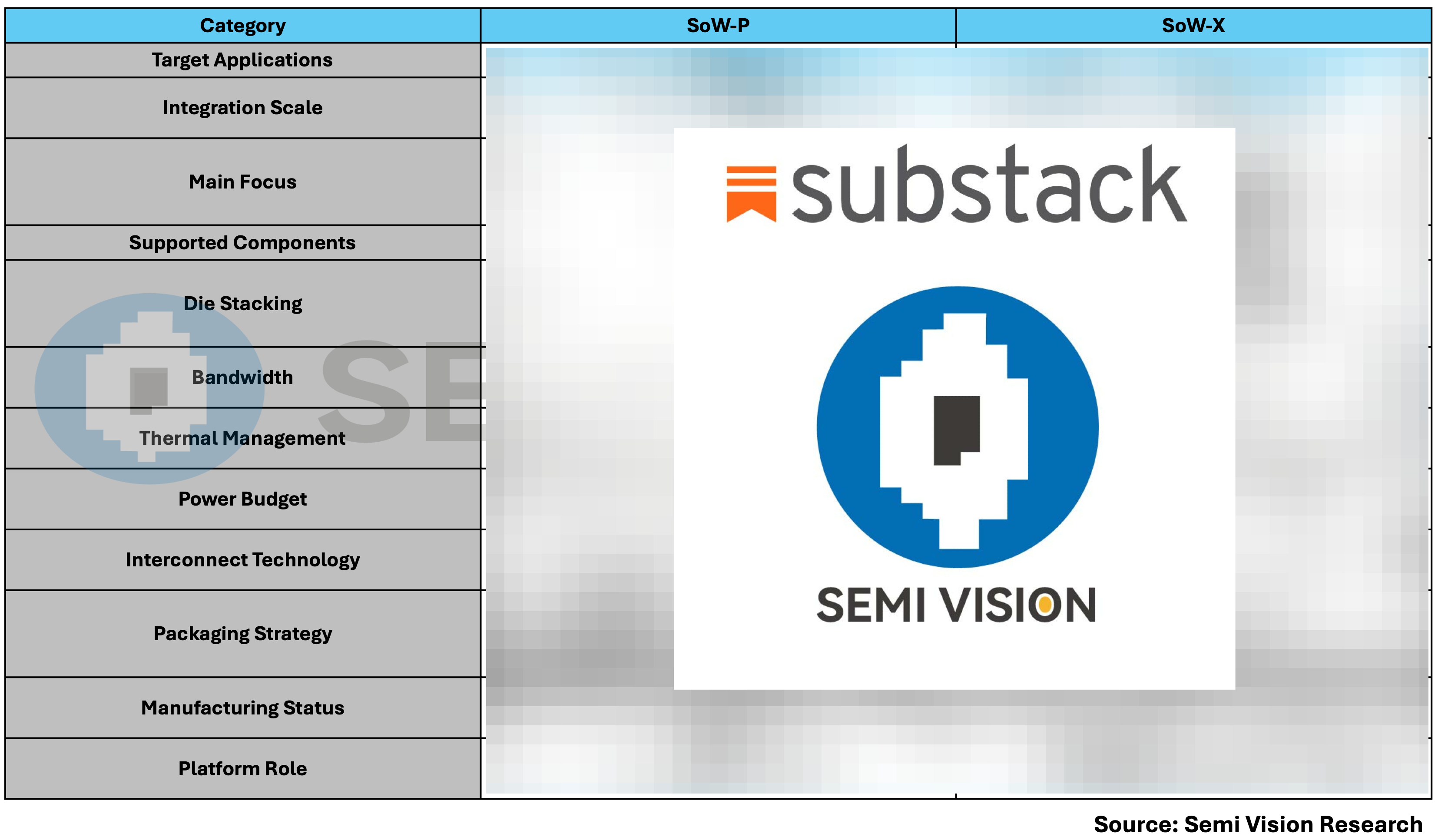
TSMC’s System-on-Wafer (SoW) technology is currently transitioning from the research and development (R&D) phase into early-stage deployment, marking a critical step forward in the fields of heterogeneous integration and ultra-large-scale packaging. This technology has evolved into two distinct platform architectures: SoW-P and SoW-X, each tailored to specific design and manufacturing requirements. These platforms are especially geared toward applications that demand extremely high compute density and bandwidth, such as Artificial Intelligence (AI) and High-Performance Computing (HPC).

For Paid Member,SemiVision will discuss topics on
Overview of TSMC’s System-on-Wafer Technologies: SoW-X and SoW-P
SoW-X: A Wafer-Scale Platform for AI and HP
System on Wafer (SoW) Technology
Application Prospects and Potential Impact
Core Value Proposition of SoW Technology
1. Reticle Size Limitation and the Rise of SoW Integration
2. Adoption of LSI and the Transition to CoWoS-L
3. InFO Family Evolution: InFO-2.5D and InFO-3D
4. Integration of IVR and PMIC
5. Thermal Budget Challenges of SoW
6. Wafer-Level Expansion of Molding Compounds
7. Innovations in Underfill Processing
8. Wafer Warpage Control
9. Optical Engine Integration into SoW
10. Innovative Assembly Design