

UMC Advanced Package Platform
Original Article by SemiVision Research

As the industry begins to better understand UMC’s long-term vision for advanced packaging, SemiVision Research participated in the Heterogeneous Package Forum 2024, a high-level industry event gathering key stakeholders including UMC, ASE Group, and several other prominent Taiwanese semiconductor players. The forum served as a strategic platform to exchange insights on the roadmap, challenges, and integration approaches for next-generation packaging and silicon photonics.

In this session, SemiVision focused particularly on analyzing the perspectives and deployment strategies of UMC and ASE, two of Taiwan’s most influential players in backend semiconductor infrastructure. While UMC shared its roadmap in enabling advanced 2.5D/3D packaging technologies—such as TSV, Fusion Bonding, and DTC (Deep Trench capacitance) platforms—ASE emphasized its leadership in fan-out, SiP (System-in-Package), and optical co-packaged integration. Both companies also addressed the increasing importance of silicon photonics in future AI and high-speed communication systems.
The discussions revealed how UMC’s positioning in both mature process platforms and emerging photonics packaging could serve as a bridge between traditional logic wafer manufacturing and new-generation heterogeneous system integration. Meanwhile, ASE continues to expand its capabilities in optical engine integration and photonic-aware packaging platforms, aiming to support customers transitioning from pluggable modules to fully co-packaged optics (CPO) and eventually to optical I/O (OIO) architectures.
This forum highlighted not only Taiwan’s depth in semiconductor packaging and photonics, but also the growing collaborative momentum across foundries and OSATs, as they prepare to address the performance, cost, and integration bottlenecks of next-generation computing systems.

SEMI Semiconductor Technology Forum Taipei 2024
On November 12, 2024, SEMI hosted the “Heterogeneous Integration and Packaging Innovation Forum” in Taipei, inviting major semiconductor equipment companies, including Grand Process Technology Corporation, UMC (United Microelectronics Corporation), ASE Group (Advanced Semiconductor Engineering), TA LIANG TECHNOLOGY CO., LTD. and CMIt to discuss challenges and solutions in advanced packaging.
Let’s first focus on UMC, which is actively advancing its development in advanced packaging technologies. UMC leverages its diverse expertise in logic chip development and integrates it with advanced packaging capabilities for broad application across multiple fields. At the recent forum, UMC’s Division Director of advanced packaging highlighted three major application areas:
1. Edge AI Inference: This includes DRAM-on-logic stacking, ideal for edge inference applications. UMC’s W2W technology is focused on integrating DRAM with logic to enable efficient, high-performance processing in edge devices.
2. Edge AI Communications: UMC is also delving into RF SOI technology, aiming to reduce RF front-end modules (RFFEM) critical form factor for enlarge the bandwidth in edge AI devices, such as 5G, 5G advanced and future 6G.
3. Edge AI Sensors: UMC took the automotive sensor as an example, particularly radar or CIS/ISP sensor applications, could leveraging advanced packaging to enhance sensor performance and integration.


These applications showcase UMC’s focus on leveraging advanced packaging to expand into fields like edge AI’s sensing, inference and high bandwidth communications, aligning with growing market demands.
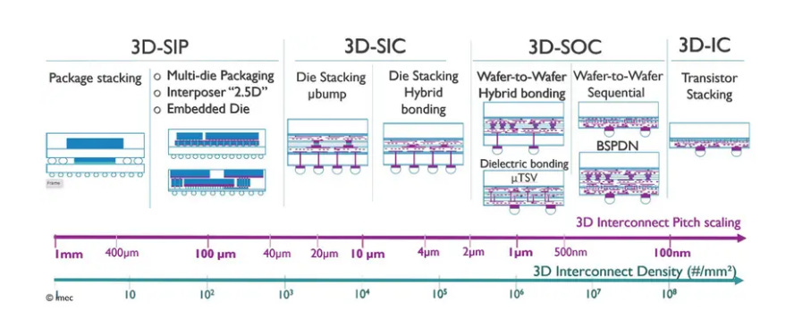
One key focus was UMC’s advanced packaging technology, which enables Wafer-to-Wafer (W2W) stacking of UMC’s logic wafers and DRAM wafers. This technology utilizes state-of-the-art hybrid bonding, eliminating the need for interconnecting solder balls, significantly enhancing logic and DRAM’s communication bandwidth. Regarding to the hybrid bonding technology, UMC seems able to support customer purchase memory house’s wafer into UMC’s logic foundry as a stacking service, according to their previous 5-way collaboration project with Faraday, Winbond, Cadence and ASE. This business model is quite different from previously we observe in the none-AI era and gives us the hint of heterogeneous fusion for future AI inferences.
Besides to the hybrid bonding technology, a critical aspect of this technology is the Through Silicon Via (TSV) process needed in the W2W stacking technology. UMC previously expanded into the so called CoWoS-S packaging with interposer solution, and the interposer solutions basically is a TSV-based process with back end of line interconnects. Additionally, UMC delved into passive component integration within CoWoS-L, a TSMC-led advanced packaging technique that centers on the Local Silicon Interconnect (LSI) wafer. The Si interposer and the LSI bridge die is essential for linking HBM with SoC, requiring custom development to incorporate passive components such as IPD (Integrated Passive Device), eDTC (embedded Deep Trench Capacitance), and IVR (Integrated Voltage Regulator).
UMC has successfully integrated eDTC (in-interposer) and discrete DTC (in LSI) into its 3DIC platform recently, marking a significant advancement in advanced packaging. This development reflects UMC’s foray into the mid-process packaging segment, with eDTC integration within the interposer or discrete DTC within LSI —an ASP-intensive process that demonstrates UMC’s commitment to advanced packaging innovations.
According to UMC’s 2024 Q3 earnings call, UMC’s current interposer production capacity stands at around 6,000 wafers per month. Looking ahead to 2025, UMC has additional trial production plans to meet potential demand increases, as customers may require more capacity. Besides its largest AI customer, UMC has a wide range of clients and projects, indicating robust demand for advanced packaging. The versatility of advanced packaging, which can be applied across numerous fields, is a key factor driving this strong demand.
In our investigation of the W2W (Wafer-to-Wafer) technology supply chain, we found that EVG Group is the primary provider, offering both Fusion Bonding and Hybrid Bonding technologies to Taiwanese foundries for advanced packaging development. Additionally, we observed that TEL and SUSS MicroTec are also making strides into the W2W field. For those interested in further technical details or the current status of advanced packaging, we welcome further discussions.

UMC’s entry into the RFSOI (RF Silicon-On-Insulator) space broadens applications to areas like antenna switch modules, LNA, and high-bandwidth 5G RF front-end modules (FEM) utilizing W2W Hybrid Bonding. This demonstrates that advanced packaging is not limited to AI computing core only, such as AMD’s MI300 series, but also finds applications across diverse sectors such as high bandwidth communication or high bandwidth sensors in the AI era. For foundries working in mature process nodes, this is a significant opportunity to leverage advanced packaging for a wider range of applications.
Finally, UMC’s advanced packaging division director exampled automotive chip applications in advanced packaging, especially as the U.S. shows signs of easing restrictions on autonomous driving. This points to growth potential in Tesla’s FSD system development, among others. A key concept shared was that while most AI chips are currently used to train large language models (LLMs) and often require advanced logic nodes like 5nm and 3nm in conjunction with advanced packaging (e.g., NVIDIA’s GB200, AMD’s MI300), there is also a growing market for AI chips used in both training and inference. Regarding to the inference in AUTO, this requires lot of high bandwidth sensors to capture the realtime information for the FSD, no matter from what kind of Radar or CIS / ISP sensor systems. To increase the sensor’s bandwidth within limited safe space per car, would require high degree of integration by either 3D W2W stacking or 2.5D interposer solutions. UMC’s advanced packaging division director noted that UMC is well-positioned to enter this space, using its advanced packaging services.

UMC’s integration of advanced packaging with its logic processes aligns with DTCO (Design Technology Co-Optimization) and STCO (System Technology Co-Optimization), adding value beyond manufacturing by offering design optimization, which enhances UMC’s role in the semiconductor ecosystem. For W2W technology, it’s crucial to focus on TSMC’s SoIC advanced process development, as future Nvidia products, like the Rubin series, may adopt a chiplet design with SoIC advanced packaging combined with CoWoS-L. This highlights the importance of K&S’s TCB Fluxless technology.

At the recent forum, ASE Group presented its VIPeak advanced packaging platform. Additionally, ASE’s CTO introduced developments in silicon photonics packaging, FAU (Fiber Array Unit) coupler technology, and CPO (Co-Packaged Optics) packaging. The memory wall effect was also discussed, emphasizing the growing importance of optical communication, which has led the industry to actively explore the feasibility of optical I/O. Here, TSMC’s COUPE silicon photonics platform is worth attention.Moving forward, we’ll provide an in-depth analysis of Grand Process Technology Corporation.and ASE Group’s Tech Talk presentations.
How to Distinguish Between CPO and OIO? What Is Their Fundamental Difference?
For Paid Members, SemiVision will provide UMC speech keynote for advanced package part
