

Unlocking the Future of Advanced Nodes.
Original Article by SemiVision Research (Dr. Yuh-Jier Mii)


At the latest technology forum, Dr. Yuh-Jier Mii, Executive Vice President of R&D at TSMC, shared the company’s leadership and latest advancements in advanced logic technology, innovations beyond A14, advanced system integration solutions, and specialty technology platforms, all centered around the vision of “Intelligence Everywhere.” Computing paradigms are undergoing a major transformation, shifting from centralized data centers to pervasive intelligence embedded across a wide range of end devices. TSMC’s advanced logic technologies, packaging innovations, and specialty platforms are positioned as critical enablers of this revolution.


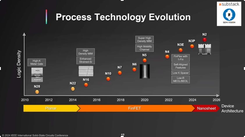
In the field of advanced logic technology, TSMC has outlined a clear and powerful roadmap. N3E entered volume production at the end of 2023, followed by N3P, which is scheduled for production by the end of 2024 with further improvements in power, performance, and density. The N2 node, recognized as the industry’s leading nanosheet transistor platform, is on track for production in the second half of 2025, achieving a consistent SRAM yield of over 90%, with accelerated adoption across mobile, AI, and HPC applications.
N2P, featuring enhanced performance and power efficiency, is planned for the second half of 2026, while N2X, targeting higher frequency requirements, is expected to enter production in 2027. Following this, the A16 node introduces the Super Power Rail (SPR) backside power delivery technology, specifically designed for data center AI and HPC applications, offering an estimated 8% speed gain or 20% power reduction at the same performance level.
Progressing further, the A14 node, based on second-generation nanosheet technology and enhanced NanoFlex Pro standard cells, aims for full-node scaling, with production targeted for 2028, delivering a 10–15% speed improvement, 25–30% power reduction, and approximately 1.23x logic density increase, followed by a SPR version in 2029.
Beyond A14, TSMC is advancing toward the next-generation device architecture. The transistor structure will transition from nanosheets to CFETs, utilizing vertically stacked n-type and p-type transistors to drive further scaling.
TSMC has demonstrated CFET inverter prototypes at 48nm and 40nm CPPs, achieving excellent electrical characteristics at voltages up to 1.2V.
Additionally, breakthroughs in low-dimensional channel materials, such as monolayer MoS₂ and WSe₂, have been achieved, laying the foundation for the future of 2D semiconductor generations. In interconnect innovation, TSMC continues to advance copper-based technologies while exploring new directions like metal etch with air gaps and intercalated graphene to significantly reduce delay and improve bandwidth efficiency.
On the system integration front, TSMC leads with its 3D Fabric™ technology portfolio. In 3D chip stacking, SoIC-P (9μm pitch) has already entered production, while SoIC-X (bump-less, 6μm pitch) is advancing toward even finer pitches, aiming for 20x more I/O density when stacking A14 on N2 platforms. In advanced packaging, CoWoS® technologies continue to expand, from CoWoS-S to CoWoS-L/R, supporting up to 9.5 reticle-sized interposers and integrating over 12 HBM stacks to meet the explosive demand for AI training capacity.
System-on-Wafer (SoW) technology takes integration even further, enabling over 40x compute expansion, with the SoW-X platform, integrating HBM and logic dies, scheduled for readiness in 2027. For future data center applications, TSMC is also developing advanced base die technologies (N12 and N3 Base Dies), silicon photonics (SiPh) interconnects, and integrated voltage regulation (IVR) solutions to meet the growing power and bandwidth demands of kilowatt-class AI GPUs.

In the specialty technology domain, TSMC continues to innovate across automotive, RF, embedded non-volatile memory (eNVM), display driver, and CMOS image sensor (CIS) applications.
Automotive customers are migrating from N7A and N5A to N3A, supporting advanced driver-assistance systems (ADAS) and full self-driving (L2+ to L4) with more than 100x defect rate (DPPM) improvement across generations.
In the RF domain, N4C RF delivers over 60% power and area scaling benefits, supporting next-generation Edge AI communication needs.
For embedded memory, both RRAM and MRAM technologies are moving toward 12nm production, with future scaling paths toward 6nm and 5nm nodes. In displays, the 16nm HV FinFET platform is enabling advanced applications such as AI glasses. Meanwhile, CIS technology advancements through LoGIC and low pixel architectures are providing unprecedented high dynamic range imaging capabilities for smartphones and ADAS.
In summary, TSMC continues to lead the industry with comprehensive advancements in logic scaling, 3D integration, materials innovation, and specialty technologies, relentlessly driving the realization of Intelligence Everywhere and collaborating closely with global customers to shape the new era of AI and the digital world.
SemiVision are providing a comprehensive keynote analysis exclusively for our Paid Members.