


OFC50: AI High-Speed Interconnect Technology Analysis by NVIDIA
Original Article by SemiVision Research (Nvidia)

Introduction: Interconnect Revolution Driven by AI

Artificial Intelligence (AI) is rapidly reshaping industries at an exponential pace. From generative AI models such as GPT and Diffusion Models to the training and inference of large language models (LLMs), the demand for computational power is imposing unprecedented challenges on underlying compute architectures and data transmission technologies.

As we enter the post-Moore’s Law and Power Wall era, performance improvements can no longer rely solely on individual chip advancements. Instead, the focus is shifting toward heterogeneous multi-GPU integration. In this context, interconnect technologies have emerged as a critical bottleneck — not only in determining system performance but also in shaping energy efficiency at scale.
Under this trend, traditional electrical interconnects, primarily based on copper wiring, are facing triple constraints:
Insufficient Bandwidth Density: In AI training clusters, data exchange often exceeds tens of terabits per second (Tbps). Copper interconnects suffer from severe signal attenuation at high frequencies, making long-distance stable transmission increasingly difficult.
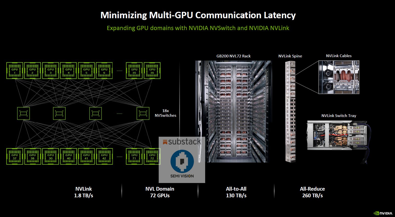
Rising Power Consumption: High-speed interfaces such as SerDes can consume 2–5 pJ/bit even over short distances, which is unsustainable for systems requiring aggregate bandwidths in the hundreds of Tbps.
Latency and Topological Complexity: AI workloads demand low-latency, real-time interconnects and memory sharing across GPUs. This places growing pressure on system topology design and modular scalability.
To address these challenges, high-speed, energy-efficient, and scalable interconnect technologies are rapidly evolving from engineering options into strategic infrastructure imperatives for data centers and AI supercomputers. These advancements span across multiple levels—from on-package GPU memory interfaces (e.g., HBM), intra-domain GPU interconnects (e.g., NVLink), to high-frequency server-to-server links (e.g., InfiniBand, Ethernet)—and extend further into packaging, photonic integration, and architectural innovation at the system level.
Emerging technologies such as Co-Packaged Optics (CPO), Linear Pluggable Optics (LPO), and Silicon Photonics are reaching commercial maturity, and in doing so, are redefining the boundaries of energy efficiency and scalability in AI infrastructure for the next decade.
Against this backdrop, the transformation of interconnect technologies is not merely a matter of technical iteration—it represents a deep industrial shift that spans packaging, materials, communication protocols, and system architecture. It is poised to become a foundational force driving the continuous evolution of AI.

For VIP Paid Members, SemiVision will discuss topics on
GPU Interconnect Architecture: System Design from On-Package Memory to Cluster-Scale Topologies
HBM On-Package Memory Network
NVLink/NVSwitch Scale-Up Network (Intra-Domain Interconnect)
Ethernet / InfiniBand Scale-Out Network (Inter-Node Interconnect)
Copper vs. Optical Interconnects: Engineering Trade-offs in the Current Landscape
The Next Step in System Design: Cross-Layer Co-Design and Ecosystem Co-Evolution
The 200G Era: SerDes, Module Selection, and LPO Constraints
LPO Design Potential and Challenges
CPO as a Complementary Solution: Addressing Long-Channel Bottlenecks
Moving Toward 400G and Beyond: From CPO to Modulator Material Innovation
The Electrical-to-Optical Interface Bottleneck: Balancing Speed and Power
Modulator Innovation: A Deep Transformation from Materials to System Integration
CPO and Interposer Optical Packaging: Breakthroughs and Limitations
Revisiting VCSEL-Based CPO: A Cost-Performance Dilemma
A Forward-Looking Roadmap for 400G/800G/1.6T Interconnects
Strategic Choices in Interconnect Technologies in future