


2025 TSMC North America Technology Symposium – Review
Original Article by SemiVision Research (TSMC Slides)

2025 North America Technology Symposium, the core topics remained largely consistent with the themes we previously analyzed—centered around the continued advancement of both process and packaging technologies. One notable deviation, however, was the absence of any in-depth discussion on CoPoS (Chip-on-Panel -on -substrate).
Further Detailed Information Presented at the 2025 TSMC Technology Symposium

As we have emphasized before, CoPoS remains in the R&D phase and is not yet part of TSMC’s production roadmap. While it holds technical promise, it still requires more time before reaching commercialization maturity.

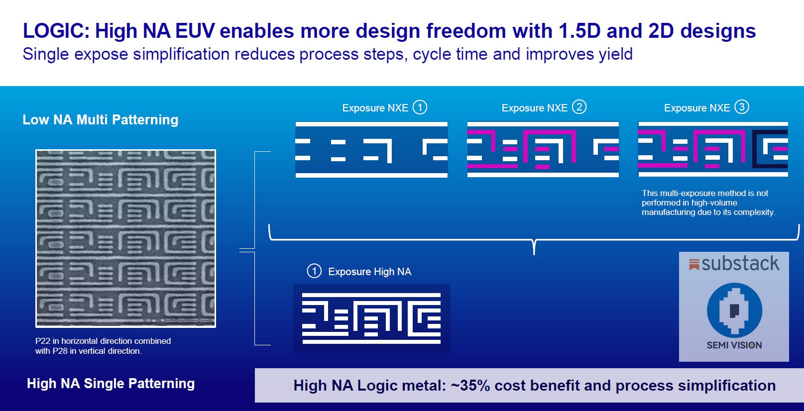
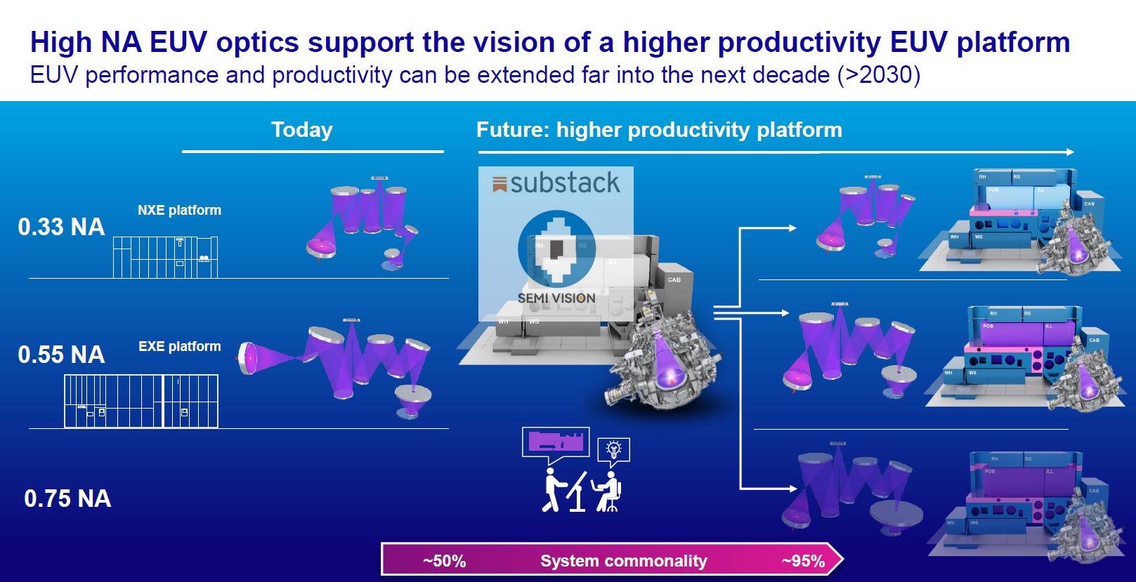
A key highlight of this year’s symposium was the introduction of A14 process technology. This aligns with our earlier forecast that post-N2 nodes would adopt a “Dual Track” strategy. TSMC confirmed that A14, representing the second generation of nanosheet transistors, will co-exist alongside A16, which features backside power delivery (SPR). What stands out in particular is the mention of High-NA EUV—a next-generation lithography technology enabling further shrinkage of pattern dimensions. This confirms that at sub-2nm nodes, TSMC is pushing boundaries not only on the logic design side, but also across the entire equipment and materials ecosystem.

Ahead of the symposium, Dr. Kevin Zhang delivered a pre-conference media briefing outlining TSMC’s latest roadmap updates and customer-driven technology directions. As a company deeply attuned to client needs, this briefing reflected insights derived from the industry’s largest semiconductor customer base.
For our Paid Members, we will deliver an exclusive summary presentation of the event with slides, including key diagrams, architectural trends, and detailed technical commentary. This will provide a deeper understanding of how TSMC is shaping its platform strategies for the next generation of semiconductor innovation.


Reconstructing the Logic Roadmap: Ecosystem Layout from N2 to A16
Technology Roadmap Extended to 2028: A14 and the Dual-Track Evolution
N3: The Final and Most Mature FinFET Node
Breakdown of Key N3 Variants
N2 Process Status and Customer Adoption
A Surge in Tape-Out Activity
A16: Nanosheet Node with Backside Power Delivery
The Dawn of the Ångström Era: A14 Launches the Second-Generation GAA Revolution
A Broadening Spectrum of Advanced Packaging Options
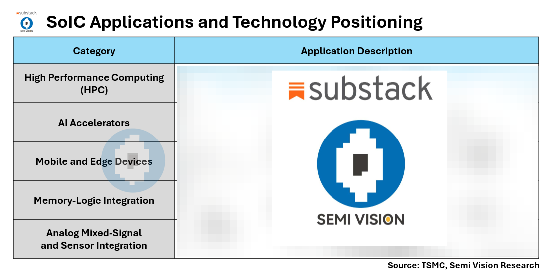
SoIC Technology: Extending Moore’s Law Through Heterogeneous Integration
Scaling Up Advanced Packaging: From CoWoS to Wafer-Level Systems
TSMC’s Integrated Power Delivery Solution for AI chip (Package ViewPoint)
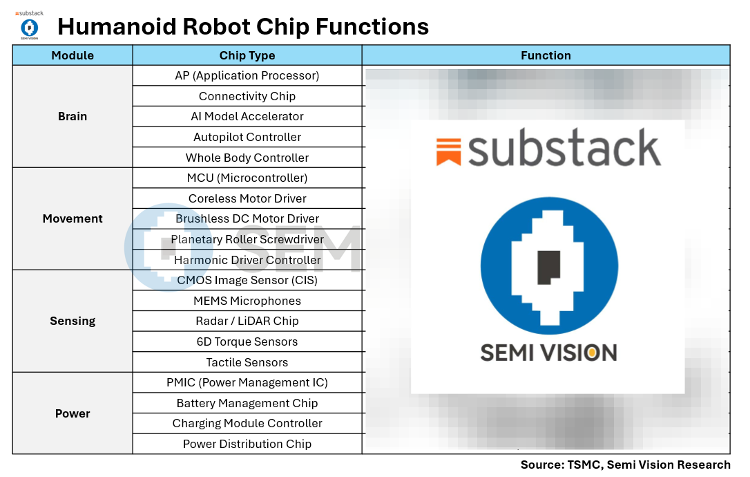
Humanoid Robots Will Define the Future of Chip Demand and Integration Technology
Synopsys and TSMC Collaboration
Industry Impact and the Future Landscape