


2025 TSMC North America Technology Symposium – Preview
Original Article by SemiVision Research (TSMC)


The 2025 TSMC North America Technology Symposium is set to begin, and based on current reports, SemiVision Research has compiled a list of key topics that are expected to be highlighted during the event. Here, we provide a brief overview of these anticipated concepts.
Topic: Advancing an AI-powered Future from Cloud to Edge


This article will be based on the foundational information presented by TSMC at 2024 IEDM.

TSMC North America Technology Symposium 2024 – Key Takeaways
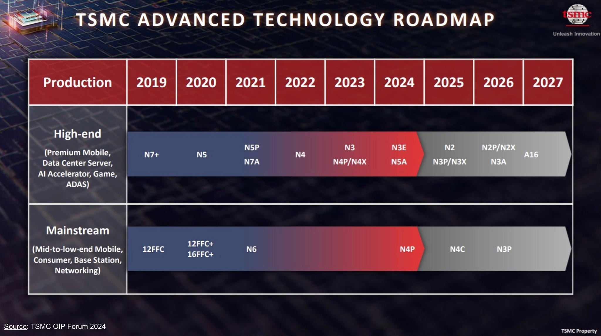
Covering critical domains such as advanced process nodes, packaging technologies, 3D IC integration, silicon photonics, and automotive applications, the 2024 forum highlighted TSMC’s continued leadership in logic scaling and platform innovation.
TSMC A16: Ushering in the 1.6nm Era of Process Leadership
As AI and high-performance computing (HPC) workloads demand ever-higher compute density and energy efficiency, TSMC officially introduced its next-generation logic platform — A16 — at the 2024 North America Technology Symposium. This node represents a major milestone in logic scaling, pushing beyond the 2nm threshold into the 1.6nm-class era, underscoring TSMC’s forward-looking strategy and R&D strength in the Beyond-2nm era.

Three-Pillar Innovation: Super Power Rail, NanoFLEX, and DCTO

The A16 platform is defined by the integration of three major innovations:
Super Power Rail (SPR):
SPR implements a backside power delivery network, moving power rails from the frontside to the wafer’s backside. This significantly reduces routing congestion and power noise while freeing up metal layers for improved signal efficiency. It marks TSMC’s first introduction of backside power in a mass-production logic node—a true generational leap in power architecture.
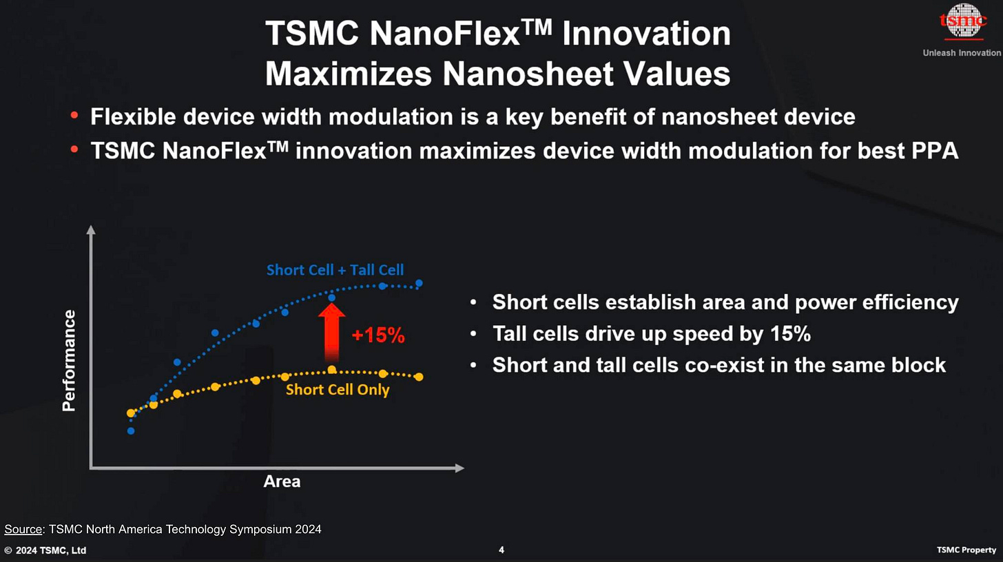
NanoFLEX Transistor Architecture:
Built on the evolution of GAA nanosheet transistors, NanoFLEX introduces flexible channel stacking, allowing the integration of different nanosheet sizes and shapes within the same design. This enables function-specific tuning—logic, memory, I/O—optimizing for performance, power, or area depending on the module, thus enhancing customization and design freedom at the transistor level.
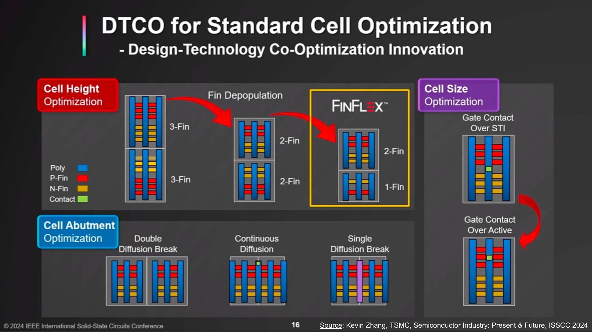
DTCO (Design-Technology Co-Optimization):
A16 fully embraces TSMC’s DTCO strategy, aligning process technology development with design enablement to optimize for PPA (Power, Performance, Area). This co-optimization accelerates design cycles, improves yield, and ensures that technology scaling translates directly into system-level competitiveness

What is DTCO?: An Introduction to Design-Technology Co-Optimization


Performance Gains vs. N2P
According to preliminary data from TSMC, A16 delivers the following improvements over the previous-generation N2P node:
+8% to +10% performance uplift
−15% to −20% power reduction
+10% increase in logic density
These metrics make A16 an extremely attractive choice for next-generation AI accelerators and HPC platforms, providing greater integration potential and energy-efficiency for complex SoC designs.


Timeline and Target Applications
TSMC confirmed that A16 will enter volume production in 2026, with targeted applications in AI accelerators, HPC systems, mobile SoCs, and high-end autonomous driving processors. It is also expected to become the foundation for future innovations in chiplet architectures, 3D stacking, and optical-electrical heterogeneous integration.
Strategic Implications: Realizing Post-Moore Architectures
In an increasingly competitive logic landscape, A16 solidifies TSMC’s leadership while signaling its readiness for the post-Moore era. While Intel promotes RibbonFET and backside power in its 18A node, and Samsung pursues multi-GAA solutions, TSMC’s A16 stands out by combining NanoFLEX scalability with DCTO platform synergy, enabling superior design flexibility and architectural integration.

A16 is not merely a shrink in node size—it represents a comprehensive transformation that bridges process innovation, design methodology, and architectural advancement. It paves the way for system-level breakthroughs and redefines what’s possible at the bleeding edge of semiconductor technology.
For Paid Members , SemiVision will discuss topics on:
N4C Process: TSMC’s Cost-Optimized Solution for the Mainstream Market
TSMC-SoW™: A New Platform for Ultra-Scale AI System Integration
TSMC 3DFabric™: The Core Platform for AI-Driven Advanced Packaging and Heterogeneous 3D Integration
3Dblox™: Design Flow Innovation for 3D IC and Advanced Packaging
TSMC Automotive Advanced Packaging and Reliability: Enabling Process Platforms for High-Safety Applications
CoPoS vs. CoWoS: The Next-Generation Packaging Shift
Dual-Track Scaling Below N2: A14 and A16 Divergence
TSMC SiliconPhotonic Platform innovation