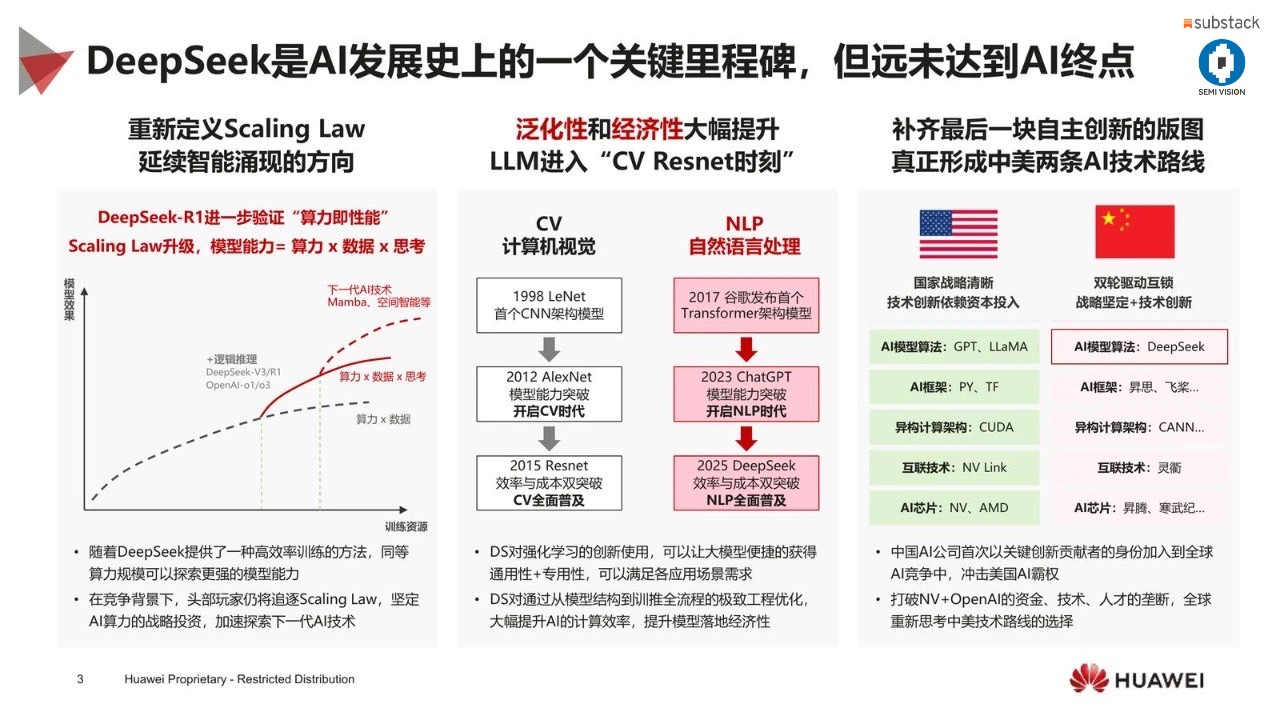
Semiconductor Manufacturing International Corporation (SMIC) has become a critical pillar in China’s push for self-sufficiency in high-end semiconductor manufacturing. As China’s largest and most advanced foundry, SMIC is at the forefront of developing AI chips that are vital for the country’s technological ambitions. According to insights from SemiVision Research, Huawei’s Ascend AI chips have demonstrated exceptional performance, positioning themselves as strong contenders against NVIDIA’s H20 AI accelerators. Ascend 910B, Huawei’s flagship AI chip, offers high training efficiency with computational performance exceeding 512 TFLOPs (FP16), optimized inference speed, and increased power efficiency due to its proprietary Da Vinci architecture. A key catalyst in this technological leap has been the emergence of DeepSeek, a leading Chinese AI model that is rapidly gaining prominence in the AI community. DeepSeek’s large language models (LLMs) and foundation models have been optimized to run on Ascend AI chips, creating a synergistic relationship that has accelerated the growth of China’s AI industry.
By aligning AI models with domestically produced hardware, China is reducing its dependence on foreign AI accelerators, ensuring greater control over its AI supply chain, and enabling faster deployment of AI applications across diverse industries, from smart cities to healthcare and autonomous driving. However, this progress is likely to escalate U.S. concerns over China’s technological autonomy, leading to stricter export controls.
The U.S. government is expected to expand the scope of export restrictions on critical semiconductor technologies, including EUV lithography, advanced GPUs, and semiconductor design tools, while also potentially limiting China’s access to AI training frameworks, cloud computing resources, and high-performance interconnect technologies essential for large-scale AI model development. The success of Ascend AI chips and DeepSeek models has positioned China as a formidable player in the global AI race, but this rapid progress is likely to provoke heightened scrutiny and control from the U.S. government, reflecting the intensifying competition in the global AI and semiconductor landscape where technological innovation and geopolitical strategy are increasingly intertwined.
NVIDIA is expected to phase out the production of its H-series AI chips at TSMC by the first half of 2025, shifting focus to the new B-series chips. According to internal sources, the transition will be seamless, with a one-to-one ratio of replacement between the H-series and B-series, ensuring no disruption in supply. The introduction of the B-series marks a significant shift in NVIDIA’s AI hardware strategy, as these new chips are expected to leverage Feynman’s architecture, which integrates cutting-edge innovations in semiconductor design and process technology. SemiVision Research has closely monitored this transition and observed that with each successive node migration to more advanced processes, NVIDIA continues to optimize for reduced leakage, lower power consumption, and increased transistor density. These improvements are critical for maintaining AI performance gains while addressing the growing challenges associated with scaling AI hardware.
At the same time, countries worldwide are strengthening their semiconductor ecosystems by injecting substantial financial resources to support domestic semiconductor industries and reduce reliance on foreign supply chains. Nations such as the United States, China, South Korea, Japan, and the European Union are ramping up investments in advanced semiconductor R&D, fabrication capacity, and AI infrastructure to secure technological leadership in the era of AI and high-performance computing. SemiVision Research has conducted in-depth analyses on these global initiatives, highlighting how government funding, coupled with private sector innovation, is driving the next phase of semiconductor growth and ensuring that countries remain competitive in the increasingly fragmented and geopolitically charged semiconductor landscape. This convergence of technological progress and strategic policy interventions underscores the critical importance of maintaining leadership in semiconductor manufacturing and AI hardware, where advancements in process technology, energy efficiency, and AI model optimization continue to shape the future of the industry.
China’s cloud computing industry is also advancing aggressively, with Alibaba and ByteDance making significant investments to expand their cloud infrastructure and AI capabilities. These efforts align with China’s national strategy to achieve self-sufficiency in semiconductor manufacturing by fostering a complete “from design to manufacturing” ecosystem that encompasses not only domestic chip design but also the development of indigenous semiconductor equipment. SemiVision Research has previously conducted a comprehensive analysis comparing China’s semiconductor equipment manufacturers with international counterparts, revealing China’s determined push to establish a robust semiconductor ecosystem. This effort aims to build an end-to-end supply chain that integrates chip design, manufacturing, and packaging into a seamless “one-stop” ecosystem that reduces dependence on foreign technology. In this context, DeepSeek, one of China’s fastest-growing AI companies, has demonstrated a strong ambition to develop its own proprietary AI chip to optimize the performance of its AI models. To achieve this, DeepSeek has collaborated with multiple Chinese ASIC design companies, seeking to customize AI chips that align perfectly with its AI workload requirements. It is highly likely that SMIC (Semiconductor Manufacturing International Corporation), China’s leading foundry, will handle the manufacturing of these AI chips, ensuring that the fabrication process remains within China’s domestic semiconductor supply chain. For advanced packaging and assembly, DeepSeek is expected to partner with leading Chinese OSAT (Outsourced Semiconductor Assembly and Test) companies, leveraging their expertise in high-performance packaging technologies such as Chip-on-Wafer-on-Substrate (CoWoS) and Fan-Out Wafer-Level Packaging (FOWLP) to maximize the efficiency and scalability of its AI accelerators. DeepSeek’s strategy to develop a proprietary AI chip not only reflects the growing trend of vertical integration among AI companies but also highlights China’s determination to control the entire AI supply chain—from semiconductor design to manufacturing and packaging. As China’s semiconductor ecosystem continues to evolve, this drive for end-to-end control will accelerate the nation’s AI advancements and solidify its position as a formidable player in the global AI landscape.
DeepSeek, one of China’s leading artificial intelligence companies, has recently made headlines with reports of its plans to develop its own AI chips, drawing significant attention from the industry. According to reports, DeepSeek has launched a large-scale recruitment effort to hire professionals in chip design, aiming to accelerate its progress in chip self-development.
Developing its own chips holds strategic significance for DeepSeek on multiple fronts. Firstly, customized hardware can optimize the efficiency of model operations, reduce energy consumption, and enhance the company’s technological self-reliance. Secondly, with the rising costs and limited availability of high-end GPU chips, in-house chip development is expected to reduce long-term expenses and improve operational efficiency.
Currently, DeepSeek has collaborated with numerous domestic AI chip companies, with its models now compatible with more than 20 Chinese AI chip manufacturers, including Huawei Ascend. Additionally, DeepSeek’s R1 modeldemonstrated impressive performance during its training process, achieving significantly lower training costs compared to its American counterparts, showcasing the company’s innovative capabilities in resource-constrained environments.
However, the path to independently developing AI chips is far from easy. It involves navigating complex stages such as architecture design, instruction set optimization, tape-out testing, and mass production. Despite these challenges, DeepSeek’s initiative is seen as a crucial step for Chinese AI companies in pursuing technological self-sufficiency. It could potentially reshape the competitive landscape in sectors such as cloud computing and intelligent devices, redefining the rules of competition in these industries.
Due to the open-source release of DeepSeek’s models, the momentum of AI development in China has been significantly boosted. As a result, many CSPs (Cloud Service Providers) are now actively collaborating with DeepSeek, fostering mutual cooperation. Currently, as many as O companies are working closely with DeepSeek to develop ASIC chips and have partnered with SMIC (Semiconductor Manufacturing International Corporation) for manufacturing.
When it comes to AI chip packaging, CoWoS (Chip-on-Wafer-on-Substrate) remains the predominant choice. We have also observed that international CSPs are making concerted efforts to develop their own AI chips, primarily to reduce costs, as NVIDIA’s chips are becoming increasingly expensive.
However, Jensen Huang (CEO of NVIDIA) has pointed out that while many companies are developing their own ASIC chips, they must also consider the ecosystem. This is where NVIDIA’s moat, CUDA, comes into play, providing a significant competitive advantage. In contrast, most CSPs still lack a proprietary ecosystem, which is why NVIDIA remains the dominant force in AI data centers.
The most talked-about topic at SEMICON China 2025 was undoubtedly SiCarrier (新凱來), whose “Mountain Series” equipment has generated intense industry interest. SemiVision Research conducted an initial analysis of SiCarrier ’s next-generation equipment lineup, highlighting their potential to advance FinFET manufacturing processes. One area that deserves special attention is the Atomic Layer Deposition (ALD) process, which will play an increasingly critical role in advanced nodes. For 2nm and beyond, the frequency of ALD steps is expected to rise dramatically, making it a pivotal component in achieving high-yield, high-performance chip production. Notably, Huawei’s key suppliers are reportedly preparing to debut a 5nm chip developed using SiCarrier’s tools, with the product line aptly named “Ali Mountain” (阿里山), underscoring the company’s confidence in its advanced equipment.
According to a Reuters report, international media have shown heightened interest in SiCarrier’s growing role in China’s semiconductor ecosystem, particularly with its contributions to advancing domestic chipmaking technology.
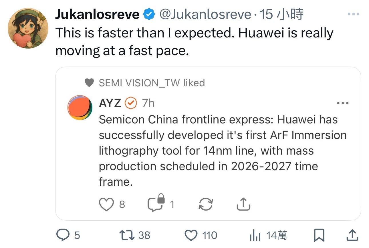
At the same time, industry sources revealed another groundbreaking development at SEMICON China—Huawei has reportedly developed its first ArF Immersion Lithography tool for 14nm production lines, with mass production expected to begin between 2026 and 2027.
According to SemiVision Research, the current lithography equipment supplier in China is SMEE (Shanghai Micro Electronics Equipment Co., Ltd.) and SiCarrier (新凱來), but in reality, its focus is primarily on DUV (Deep Ultraviolet) lithography technology.
This milestone marks a major step toward China’s semiconductor self-sufficiency, as immersion lithography is critical for producing advanced nodes below 28nm. Huawei’s achievement signals a potential shift in the global lithography landscape, as China accelerates efforts to develop indigenous lithography solutions that could reduce reliance on foreign suppliers. The combination of SiCarrier’s advanced deposition equipment and Huawei’s breakthrough in immersion lithography suggests that China is building a robust, vertically integrated semiconductor supply chain, capable of supporting cutting-edge chip manufacturing and positioning itself as a formidable player in the global semiconductor market.
SemiVision Research believes that while China has made some progress in DUV (Deep Ultraviolet) lithography and EUV (Extreme Ultraviolet) lithography, its breakthroughs have primarily been in the light source segment. However, the complexity of lithography equipment goes far beyond just the light source, requiring advancements across multiple domains. For instance, ASML’s EUV lithography machine is one of the most sophisticated and precise pieces of equipment in modern semiconductor manufacturing. Each EUV machine consists of over 100,000 individual components, including 3,000 wires, 40,000 bolts, and 2 kilometers of tubing. Once fully assembled, the machine is about the size of a small bus and weighs between 150 to 180 tons. Due to its massive size and intricate design, these machines are typically disassembled into around 250 separate crates for transportation, including 13 large shipping containers. These details highlight the extreme complexity and precision involved in designing and manufacturing EUV lithography equipment.
In addition to the challenges related to the machine’s physical structure, the optical system of the EUV lithography machine presents another formidable hurdle. ASML’s EUV machines rely on an advanced multilayer reflective mirror system developed by Zeiss, with precision at the nanometer level. Each of these mirrors must maintain surface errors below 0.1 nm to ensure accurate reflection of the EUV light, a level of optical precision that remains beyond China’s current technological capabilities. Moreover, the light source used in EUV lithography is generated by tin (Sn) plasma, producing 13.5nm wavelength extreme ultraviolet light, which requires extremely high power inputs to maintain a stable exposure process. Additionally, the system operates in a high vacuum environment, making the development of a domestic EUV machine in China exceptionally difficult. Even if breakthroughs are achieved in light source technology, China would still face a series of challenges related to optical systems, mirror fabrication, precise motion control, and maintaining ultra-high vacuum conditions. Therefore, developing an indigenous EUV lithography machine will require prolonged technological accumulation and industrial collaboration.
On the other hand, photoresist is another critical component that poses challenges for domestic lithography efforts. EUV photoresists must offer higher resolution and better etch resistance, while perfectly matching the wavelength of EUV exposure. Currently, the high-end photoresist market is dominated by companies such as JSR, TOK, Sumitomo Chemical, Shin Etsu, Fujifilm in Japan, and Dupont in the United States. Although China has made progress in the field of photoresists, it will take a considerable amount of time and close collaboration with suppliers to optimize these materials to meet the demands of EUV lithography.
As a result, SemiVision Research believes that while China has made some advancements in DUV lithography, developing an EUV lithography machine remains a formidable challenge that cannot be overcome in the short term. DUV lithography is a more feasible option for China, but even in this domain, success requires more than just a single technological breakthrough. It necessitates a comprehensive ecosystem and technological integration across multiple domains, including light sources, optical systems, photoresists, precision motion control, and vacuum environment maintenance, to achieve true competitiveness in lithography equipment. Therefore, while China can continue to make steady progress in DUV technology, achieving a breakthrough in EUV lithography will require much more time, technological accumulation, and continuous improvements in supply chain and ecosystem integration to narrow the gap with ASML.
For Paid Members, SemiVision Research will discuss following topics