

Decoding Node Strategy: MediaTek’s Long-Lasting Process Nodes and AI Roadmap
Original Articles By SemiVision Research (MediaTek , TSMC , Nvidia , AWS , Google , Ranovus , Alphawave Semi ,Xanadu , AMD , Cerebras )

From Chip Definition to System Integration: MediaTek at the Crossroads of Advanced Packaging
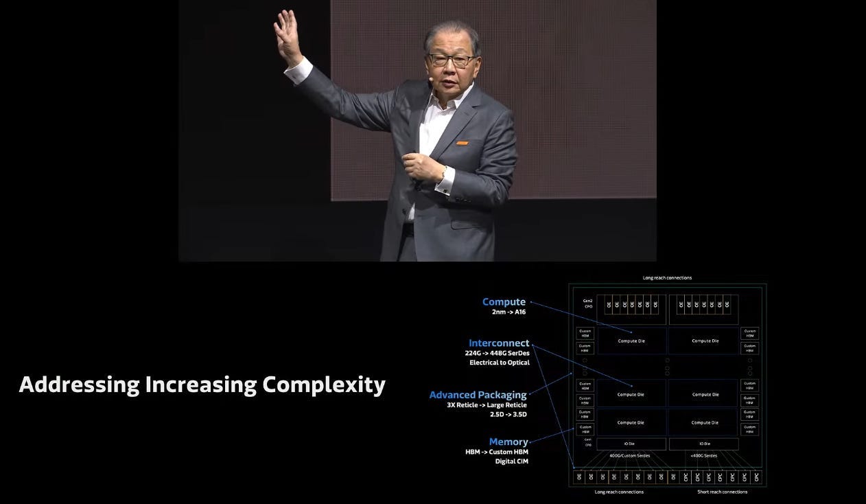
In the era of AI-driven performance-per-watt optimization and heterogeneous integration, the nature of chip design is shifting—from a singular focus on computational horsepower to a packaging-centric, system-level co-design paradigm. Under the traditional Moore’s Law trajectory, the interplay between performance, power, and cost (PPC) is increasingly challenged beyond the 7nm node. While advanced nodes still offer advantages for specific applications, escalating manufacturing costs, slower SRAM scaling, and diminishing cost-per-transistor improvements are forcing the industry to seek new performance uplift curves. Advanced packaging has emerged as the key enabler to transcend the limitations of traditional node scaling.

As a global leader in IC design, MediaTek has evolved from its consumer electronics SoC roots to expand into Edge AI, ASICs, and automotive markets. In doing so, it has increasingly recognized advanced packaging not merely as a manufacturing consideration, but as a strategic capability. This evolution touches not only how chips are architected and IPs are integrated, but how system-level synergy across performance, thermal design, and power consumption can be fully optimized.
Extension|MediaTek’s Advanced Packaging Strategy Through the Lens of ASIC Evolution
As MediaTek enters the ASIC domain, its role shifts from a provider of high-integration SoCs to a collaborative development partner for application-specific and vertically integrated solutions. In AI servers, voice assistants, and edge computing, MediaTek co-creates highly customized designs with clients—driving up the demand for packaging technologies that enable flexibility, integration, and reliability.
MediaTek clearly recognizes that in a landscape where GAA nodes remain immature (TSMC’s 2nm GAA process is still cost-prohibitive), and FinFET gains are tapering off, the ability to leverage CoWoS, EMIB, or more adaptable RDL and glass substrate packaging will directly impact the commercial viability of ASIC solutions—especially in terms of bandwidth, thermal management, and yield.
Unlike traditional consumer-grade chips that chase economies of scale, ASICs and Edge AI emphasize packaging flexibility and modularity. As such, MediaTek is focusing on several key packaging trends:
2.5D/3.5D Heterogeneous Integration: Leveraging architectures such as CoWoS-L and CoWoS-R to integrate AI accelerators, SerDes, and HBM onto a single packaging platform;
Yield-Driven Packaging Selection: Choosing long-tail nodes and mature packaging (e.g., organic substrates with embedded silicon bridges like EMIB) to manage BOM costs and reduce ramp-up complexity;
Co-Design in Packaging Simulation and System Optimization (DTCO, STCO): Engaging in early-stage thermal, power, signal integrity, and mechanical stress simulations to reduce development time and ensure manufacturing stability;
Adoption of Glass Core Substrates: For applications requiring superior warpage control and electrical performance, glass substrates are emerging as a transformative next-generation option.
In summary, as MediaTek advances into the ASIC and high-end Edge AI domains, it is no longer just a traditional chip vendor. It is becoming a system integrator, using advanced packaging as a strategic platform to meet new expectations in AI, connectivity, and automotive markets. With increasing demand for energy efficiency and modular scalability, advanced packaging is poised to be a key differentiator and a gateway for MediaTek’s entry into high-value markets.

From Smartphones to AI Chip Design Services: MediaTek’s Strategic Shift and Process Technology Strategy
At the 2025 IEEE VLSI Symposium panel discussion, MediaTek clearly articulated its transformation from a consumer SoC provider to a critical solution partner in the AI era. The discussion revealed that MediaTek is no longer confined to smartphone APs and voice assistant platforms—it is now actively providing SerDes IP and offering design services for cloud service providers (CSPs) developing AI chips, marking a pivotal step in its evolution.
This article begins by examining MediaTek’s transformation and delves into its logic process technology strategy, evolving ASIC design philosophy, and long-term vision for advanced packaging.
1. MediaTek’s Transformation: From SoC Supplier to AI Chip Partner
Over the past decade, MediaTek has built strong SoC integration capabilities across smartphones, TVs, and IoT markets. In the AI era, the company has shifted toward AI-centric chip design, particularly in voice assistants, edge AI, and AI accelerators—offering customized, system-oriented solutions.
A key milestone in this transformation is MediaTek’s growing investment in high-speed SerDes IP. Originally developed for internal SoC interconnects, SerDes capabilities are now supporting CSP clients in high-performance AI training chips, enabling fast interconnects with HBM, switch chips, and other components. This has become a critical foundation for MediaTek’s AI chip design services.
2. Logic Process Strategy: Balancing Advanced and Mature Nodes
At the panel, MediaTek emphasized the importance of flexible process node selection, stating that different application scenarios require different co-optimization approaches under its in-house DTCO framework (Design-Technology Co-Optimization):
For high-performance AI training/inference chips, MediaTek evaluates nodes like TSMC N3 or N2 based on transistor density, power efficiency, and compatibility with SerDes voltage requirements. While GAA offers better drive current, its high cost and design complexity must be carefully assessed.
For edge AI and mid-performance applications, mature FinFET nodes such as N6/N12 are often preferred. These are combined with modular packaging techniques (e.g., RDL, EMIB) to deliver a balanced solution in terms of bandwidth and power.
This “application-driven process selection” signals a fundamental shift from performance-centric SoC thinking to a system-level integration mindset.
3. A Packaging-Centric Approach: From Chip Modules to System Platforms
As chip performance becomes increasingly constrained by interconnects and packaging, MediaTek is actively developing integration strategies focused on advanced packaging technologies. Its key approaches include:
2.5D integration (e.g., CoWoS-L): For high-performance AI ASICs that require HBM and multi-die logic integration.
EMIB bridging: Combining mature-node logic designs with high-speed SerDes to achieve cost-effective, high-bandwidth packaging.
RDL modular packaging: Supporting flexible IP configurations and promoting the concept of “package as system.”
Adoption of glass core substrates: Addressing needs for warpage control and electrical performance—particularly relevant for automotive AI and high-speed communication ASICs.
Furthermore, MediaTek highlights that DTCO and STCO (System-Technology Co-Optimization) are critical to future adoption of 3D ICs and chiplet architectures.
4. From Smartphone-Driven SoCs to Packaging-Defined AI Platforms
MediaTek now stands at the intersection of logic design, system packaging, and IP integration. Its role is evolving from a chip supplier to a packaging-centric system design partner. This transformation enables MediaTek to carve out a differentiated position in the increasingly competitive markets of AI ASICs and Edge AI solutions.

As CSPs, automotive OEMs, and next-generation manufacturing industries demand higher energy efficiency, bandwidth, and modularity, MediaTek’s continued progress in packaging architectures, process co-design, and IP collaboration will determine its long-term value in the AI infrastructure landscape.
In the AI-driven wave sweeping across the semiconductor industry, MediaTek is no longer just the silent champion of mobile SoCs—it is emerging as a key enabler powering voice assistants, smart homes, AI tablets, and intelligent edge devices. While much of the industry remains fixated on cloud-scale model training and hyperscale compute, MediaTek is quietly building a device-centric AI empire through ASIC development, advanced packaging, and long-lifecycle process node strategies.
From PoP memory architectures to 2.5D/3D heterogeneous integration, from ultra-low-power neural inference for voice agents to its strategic use of TSMC’s N3E as a long-lasting node in the GAA era—every step MediaTek takes is not merely a technical decision, but a calculated balance of design flexibility, cost optimization, and system efficiency.

In the evolving global semiconductor innovation landscape, Canada is increasingly showcasing its technological potential and industrial competitiveness. Beyond its long-standing foundation in quantum computing and photonics research, recent years have seen a surge of startups actively engaging in Silicon Photonics, Advanced Packaging, Co-Packaged Optics (CPO), custom AI ASICs, and Lithium Niobate on Insulator (TFLN) technologies. These developments are gradually shaping a regionally distinct semiconductor innovation ecosystem in Canada.
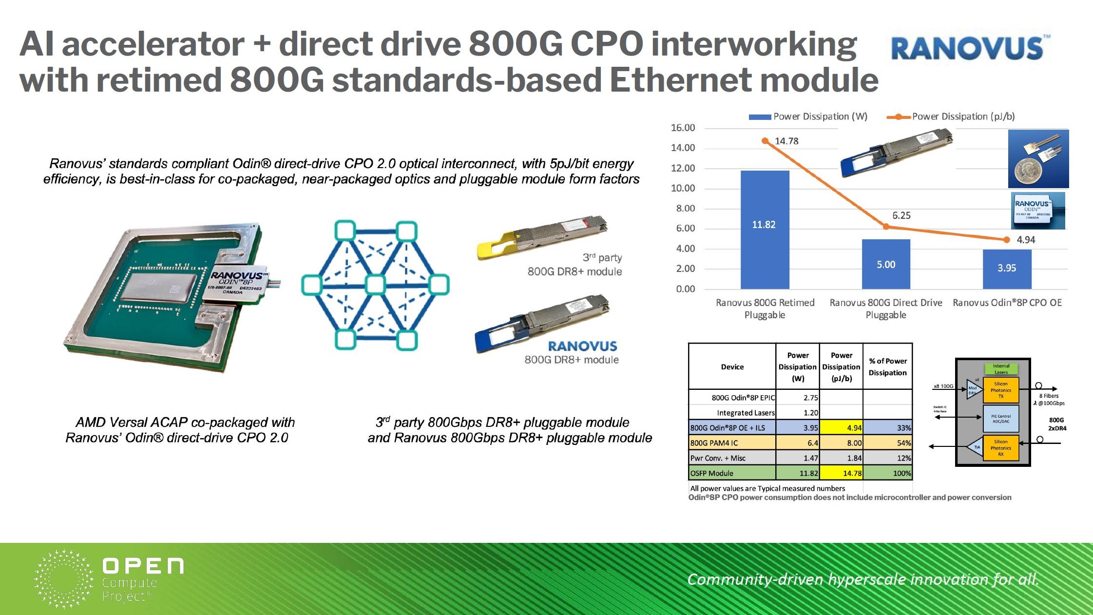
Among them, Ranovus stands out as a prominent player. Headquartered in Ottawa, the company specializes in modular CPO optical engines and EPIC (Electronic-Photonic Integrated Circuit) platforms. Ranovus has already established partnerships with leading global semiconductor companies such as AMD, Cerebras, and MediaTek. Its Odin® optical engine, now in mass production, supports high-speed DWDM transmission and offers advantages in low power consumption and high integration. Ranovus is one of the few startups globally to have successfully entered the commercial deployment phase of CPO technology.
New innovations in hybrid Silicon Photonics and TFLN platforms are accelerating globally. These technologies aim to integrate high-speed lithium niobate (LN) modulators into CMOS-compatible photonic platforms, addressing critical bottlenecks in bandwidth and process compatibility for data center and LiDAR applications. Many countries around the world are actively investing in the next generation of TFLN-based technologies. In particular, Europe has produced a significant body of academic research exploring TFLN applications. At the same time, China has emerged as one of the fastest-growing regions in terms of TFLN development, with rapid advancements in both research and commercialization.

Alphawave Semi, formerly known as Alphawave IP and also based in Toronto, has gradually evolved into a publicly listed company. It originated in the fields of SerDes, optical interconnects, and custom ASIC architectures, and continues to develop advanced packaging solutions supporting UCIe, CXL, and chiplet-based system integration through its Canadian R&D center.
Additionally, companies like Xanadu, which focus on optical quantum computing, are pushing boundaries. While primarily centered on quantum information, Xanadu’s silicon photonics platform and fabrication technologies are increasingly converging with the broader semiconductor supply chain, particularly in TFLN materials and hybrid bonding innovations.
In summary, Canadian semiconductor startups are emerging as key innovators, leveraging core themes such as photonics-electronics convergence, high-bandwidth interconnects, CMOS-compatible processes, and heterogeneous integration to tap into next-generation global semiconductor competition. This growing ecosystem is one that should not be overlooked.

MediaTek Partners with Ranovus: Advancing into the High-Performance AI Chip Era with Co-Packaged Optics (CPO)
As AI and HPC workloads scale exponentially, bandwidth and power efficiency have emerged as the primary bottlenecks in expanding system architectures. To strengthen its system integration capabilities in AI ASIC design, MediaTek announced a strategic partnership in 2024 with Canadian photonics company Ranovus. Together, they aim to co-develop next-generation Co-Packaged Optics (CPO) solutions, injecting high-efficiency optical interconnect technologies into future AI chip platforms.

A Modular CPO Platform: System Design Breakthrough by MediaTek × Ranovus

MediaTek’s new-generation ASIC design platform integrates its proprietary 112Gbps SerDes technology with Ranovus’ Odin® optical engine, achieving a highly modular electro-optical integration. This platform supports 8×800Gbps electrical and optical channels, featuring low power consumption, high bandwidth, modularity, and reconfigurability. Not only does this significantly reduce PCB routing complexity and packaging footprint, but it also cuts overall system power consumption by up to 50%, providing an economically viable high-speed interconnect solution for AI data centers and large-scale inference systems.
This collaboration marks MediaTek’s strategic transition from mobile SoC design toward data center-class AI platforms, pushing its chip design and packaging integration capabilities to meet next-generation bandwidth and energy efficiency demands.
Ranovus: A Pioneer in AI Optical Interconnects
Ranovus, headquartered in Ottawa, Canada, is a leading player in optical interconnect solutions. The company offers a comprehensive platform including Quantum Dot Lasers, integrated Electronic-Photonic Integrated Circuits (EPIC), and high-density CPO modules. Its Odin® series delivers power efficiency as low as 4pJ/bit and supports over 6.4Tbps of bandwidth, making it one of the most advanced CPO modules in the industry.
Ranovus’ core strength lies in its high level of integration, production-ready design, and close ties with global foundry and packaging supply chains, enabling it to rapidly support system vendors in building commercial-grade CPO platforms.
Collaborations with AMD, MediaTek, and Cerebras
In addition to MediaTek, Ranovus has formed strategic partnerships with several leading semiconductor companies:
AMD/Xilinx: Ranovus previously demonstrated its Odin 2.0 platform integrated into AMD’s FPGAs and AI acceleration chips, targeting AI/ML edge computing applications.
Cerebras Systems: In 2025, Ranovus and AI chipmaker Cerebras jointly secured a DARPA contract to implement optical interconnects into Cerebras’ wafer-scale systems, supporting ultra-large-scale AI training.
These collaborations underscore Ranovus’ role as a core enabler of cross-platform, cross-application optical interconnect deployment, with proven technical versatility and execution.
MediaTek’s Strategic Intent Behind CPO
For MediaTek, the partnership with Ranovus carries three strategic implications:
Rapid Entry into the High-Bandwidth Interconnect Market: Leveraging Ranovus’ mature platform, MediaTek can quickly build CPO module development and validation capabilities.
Enhancing the Completeness of its AI ASIC Platform: MediaTek moves beyond providing compute cores to offering a fully integrated solution encompassing IO, SerDes, optical modules, and packaging.
Alignment with High-End Supply Chain Players: Co-development with Ranovus and TSMC strengthens MediaTek’s influence in advanced packaging and system-level integration.
The MediaTek–Ranovus partnership is more than just a technical alliance—it signals the entry of Taiwanese IC design houses into the core battlefield of high-bandwidth, low-power AI/HPC data center platforms. As AI models continue to grow in scale and CPO becomes central to future system architectures, MediaTek’s bold move is poised to fuel its next phase of growth across data centers, cloud infrastructure, and AI chip markets.
In this SemiVision Technical Special, we unpack seven strategic pillars of MediaTek’s platform play—spanning FinFET-to-GAA packaging transitions, SRAM bottleneck solutions, edge AI SoC architecture, and how N3E has become the modern definition of a long-lifecycle node. Each topic dives deep not only into the underlying technologies but also the broader system-level logic and supply chain implications.
If you care about the evolution of edge devices in the AI era, the real value of advanced process nodes like N3E, or are looking to differentiate through packaging and heterogeneous integration—this is the article you cannot afford to miss.
Unlock the full story and discover how MediaTek is quietly becoming the most strategic “system player” in the AI age.
For Paid Members , SemiVision will discuss topics on
The Long-Term Evolution of Process Nodes: Key Inflection Points Behind Each Generational Leap
The Four Driving Forces Behind Technological Leaps: Materials, Lithography, Patterning, and Device Architecture
Platform Nodes and System-Level Integration: The Decision Matrix for IC Design Houses
Strategic View: Process Evolution as a Platform-Driven Race
The Node You Choose Is the Platform You Build On
From Node Scaling to Platform Strategy: The Logic of Long-Lived Nodes and the Strategic Role of TSMC N3
N3: TSMC’s Modern Definition of a Long-Lived Node
Process Scaling Is Guided by a Rhythm of Long-Lived Nodes
The Concept of the “Process Universal Curve”
The Evolutionary Trend of Advanced Process Nodes in Performance and Power — The “PP” in PPA
Area Scaling Trends in Advanced Process Nodes: The Bottleneck of SRAM Miniaturization
Transistor Cost Reduction in Advanced Nodes: Slowing Down and Facing Reversal at 2nm and Beyond
The Bottlenecks and Transformation of Moore’s Law in the Sub-7nm Era
MediaTek Joins Forces with Google: Strategic Entry into TPU Design and Its Future Implications
2.5D and 3.5D Advanced Packaging Architectures: Comparing TSMC’s CoWoS and Intel’s EMIB
Future Scalability of CoWoS and EMIB in Heterogeneous Integration Packaging
A Critical Inflection Point in Core Substrate Materials for Advanced Packaging
Scaling Advanced Packaging: Multidimensional Challenges and the Rise of Glass Substrates
SemiVision Technical Insight Series: Unpacking MediaTek’s Innovation Across Seven Strategic Dimensions
1.MediaTek’s Strategy and Challenges in Advanced Packaging: CoWoS, EMIB, CPO, and Glass Substrates
2.Collaboration Between MediaTek and NVIDIA on AI ASIC and NVLink Technologies
3.Differentiating Products Through Advanced Packaging: MediaTek’s Path into Cloud AI and HPC
4.Automotive Market Strategy: 3nm DX1 Platform, 5G Cockpit Integration, and Packaging Challenges
5. Edge AI Product Line: GB10 and Multi-Agent (MCP/A2A) Architecture Enabled by Advanced Packaging
6. Packaging Challenges and Solutions in the FinFET/GAA Era: PPA Optimization, SRAM Bottlenecks, and Cost Control
7. End Applications: Voice Assistants, Smart Home, and AI Tablet Strategy — Empowered by Advanced Packaging and AI ASIC Integration
