

EMIB Meets Photonics: Building Reliable CPO for Zettascale AI Networks
Original Article by SemiVision Research (IEEE ECTC , Intel )

The emergence of Silicon Photonics is reshaping AI chip architectures. One of the most discussed topics is how to integrate Silicon Photonics into Optical I/O (OIO) systems, particularly by embedding optical engines directly onto the interposer. We have already seen TSMC outline a roadmap in this direction, mainly driven by considerations for NVIDIA’s future needs.
Our previous articles have introduced several foundational concepts—such as FAU (Fiber Array Unit), 2D Grating Coupler (GC), and even System-on-Wafer (SoW) integration. Now, we’re seeing that Intel is pursuing a similar vision. They are integrating EMIB (Embedded Multi-die Interconnect Bridge) technology with optics, and this paper highlights several key areas:
How advanced packaging can be integrated with optical components
The relationship between FAU arrays and connector design
Reliability testing, including for optical fibers and photonic components
A technical summary of Intel’s CPO fiber packaging and testing flow
The design of fiber array unit connectors and optical coupling mechanisms
There were numerous papers on Co-Packaged Optics (CPO) at the 2025 IEEE ECTC. Moving forward, the SemiVision team will continue to analyze the CPO technologies presented at ECTC. For this update, we’ll start by discussing Intel’s CPO solution.

Intel’s development of silicon photonics represents over two decades of dedicated innovation and progress, gradually paving the way for a new era of electro-optical convergence in high-performance computing and data centers. Since 2000, Intel has been investing in silicon photonics research, tackling the inherent challenge that silicon cannot emit light on its own. By leveraging heterogeneous integration technologies, Intel successfully incorporated high-performance III-V materials (such as InP) into silicon chips, enabling the creation of hybrid silicon lasers. In 2004, the company demonstrated high-speed silicon optical modulators, laying the technological foundation for high-speed optical communication.
As the technology transitioned into commercialization, Intel introduced its first 100G PSM4 silicon photonics optical module in 2016. This module offered high-speed, low-power optical interconnects for hyperscale data centers. Utilizing wavelength division multiplexing (WDM) to increase data throughput, Intel’s solution quickly became a vital enabler in cloud and compute infrastructure.

As AI and HPC applications continue to drive unprecedented demands for bandwidth and energy efficiency, Intel took a significant step forward in 2020 by advancing its efforts in Co-Packaged Optics (CPO) architecture.

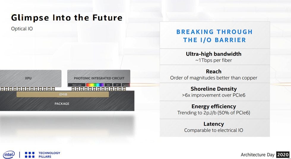
In 2024, Intel unveiled the world’s first prototype design integrating an Optical I/O chiplet, achieving up to 2 Tbps of bidirectional data throughput while reducing power consumption to approximately 5 picojoules per bit. This architecture emphasizes the direct integration of photonic integrated circuits (PICs) and electronic driver chips (EICs) within the ASIC package, significantly shortening signal transmission paths, lowering latency, and improving overall energy efficiency.

This image showcases Intel’s Co-Packaged Optics (CPO) demonstration at OFC 2024, highlighting a real-time optical data transmission setup between two systems—System 1 and System 2—connected via single-mode optical fibers. In this demo, System 2’s optical transmitter (TX) sends PRBS-31 test data to System 1, while the optical spectrum of 8 wavelengths per fiber (with 200 GHz spacing) is displayed on a spectrum analyzer. System 1 receives the data through its optical receiver (RX), performs bit error rate (BER) analysis, and captures the transmitted eye diagram on a real-time oscilloscope. The BER plot in the center illustrates performance across multiple lanes under various control settings. This demonstration validates the high-speed optical signaling capability of Intel’s Optical I/O chiplet integrated directly into CPU packages, showcasing Intel’s advancement in photonic-electronic co-packaging and wavelength-division multiplexing (WDM) transmission.
Looking ahead, Intel is expanding its silicon photonics platform into a broader range of applications, including 5G fronthaul, LiDAR, and high-bandwidth interconnects. The company is also planning to advance its photonic modules to support 200G per channel, enabling 800G and 1.6T system architectures. This strategic roadmap not only underscores Intel’s long-term commitment to photonic technologies but also steadily reinforces its leadership in the fields of co-packaged optics (CPO) and photonic-electronic integration.

For Paid Members, SemiVision will discuss topics on
Silicon Photonics: Unlocking Cross-Domain Innovation Potential
1. Data Centers and High-Performance Computing (HPC)
2. Artificial Intelligence (AI) and Machine Learning
3. Quantum Computing
4. Sensors and LiDAR
5. Optical Communications and Free-Space Optics (FSO)
6. Portable Devices and Consumer Electronics
Intel’s Advanced Packaging Innovations: Integrating Optics with EMIB Technology
Why is “Fiber-based CPO + EMIB” so critical?
From Assembly to Testing: A Roadmap to High-Volume Manufacturing (HVM)
Reflow and Reliability: Tackling JEDEC-Level Challenges
Building the Optical Interconnect Infrastructure for the AI Era
Connector Design and Optical Coupling Mechanism for Fiber Array Units
Packaging Architecture: MCP Structure and Heterogeneous Integration
Intel OIO Solution
Overview of Fiber Array Unit (FAU) Design and Packaging Configuration
Intel CPO Optical Fiber Packaging and Test Flow Summary
