Intel’s Next Frontier: Redefining Chiplet Integration Through Advanced Packaging
Original Article by SemiVision Research (Intel , TSMC , Nvidia)

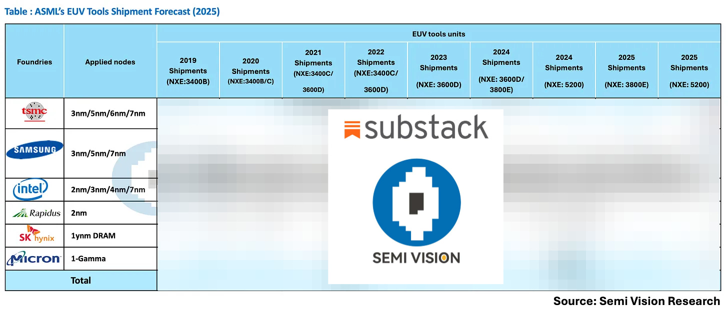
Most people’s understanding of advanced packaging tends to center around TSMC’s 3DFabric platform, but currently, TSMC, Samsung, and Intel are the main foundries offering advanced packaging platforms.

For readers interested in Intel’s technology, you may refer to the following articles.


Before we can fully understand Intel’s logic behind its process node naming, we must first recognize its strategic shift—from an IDM (Integrated Device Manufacturer) to a foundry model under Intel Foundry Services (IFS)—and how this impacts its competitive positioning in the advanced process market. In particular, for the 18A and 14A nodes, Intel has adopted technical standards and marketing definitions that differ significantly from TSMC’s approach.


Intel 18A: The Key Node Featuring RibbonFET and PowerVia
Intel’s 18A process node marks its first full integration of GAA (Gate-All-Around) transistor architecture, which Intel calls RibbonFET, along with backside power delivery, known as PowerVia. This generation of process technology represents Intel’s complete departure from the FinFET era, moving toward a design that enables higher drive current and improved power integration.

It’s worth noting that Intel has not treated 18A as a single monolithic node, but has instead introduced two derivative sub-nodes:
Intel 18A-P: An extension of the original 18A platform, likely featuring process refinements or parameter optimizations tailored for specific IPs.
Intel 18A-PT: A further enhanced version, potentially indicating support for higher-density designs or the early adoption of pre-research technologies from the upcoming 14A node.

When compared to TSMC, Intel’s 18A is roughly equivalent to TSMC’s A16 node—which refers to TSMC’s 2nm-class GAA + backside power delivery architecture, expected to be implemented using its Super Power Rail (SPR) technology.
Comparison and Differentiation Between Intel 14A and TSMC A14
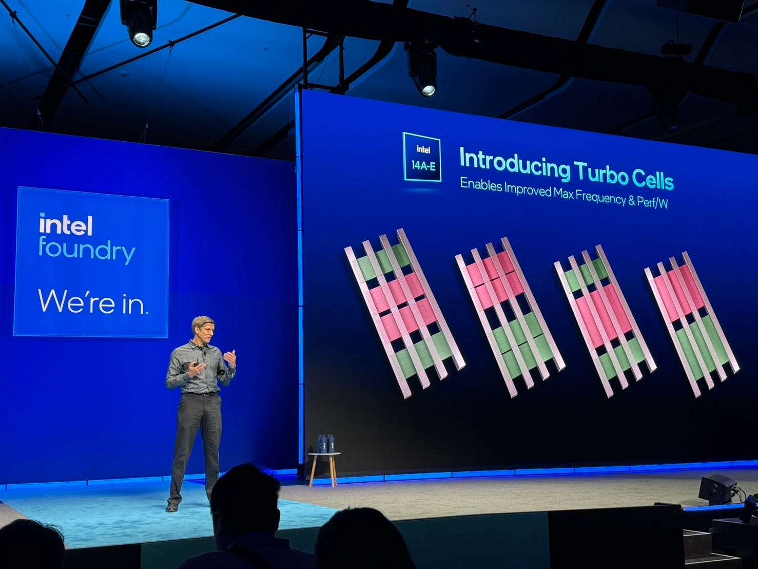
At the end of 2024, Intel officially unveiled its next-generation process node—Intel 14A—positioned as the technological successor to 18A. It continues the use of RibbonFET and PowerVia architectures while enhancing design rules and transistor density. Intel also introduced a variant called 14AE (14A Enhanced), suggesting potential optimizations for specific markets such as AI, 5G, and HPC.
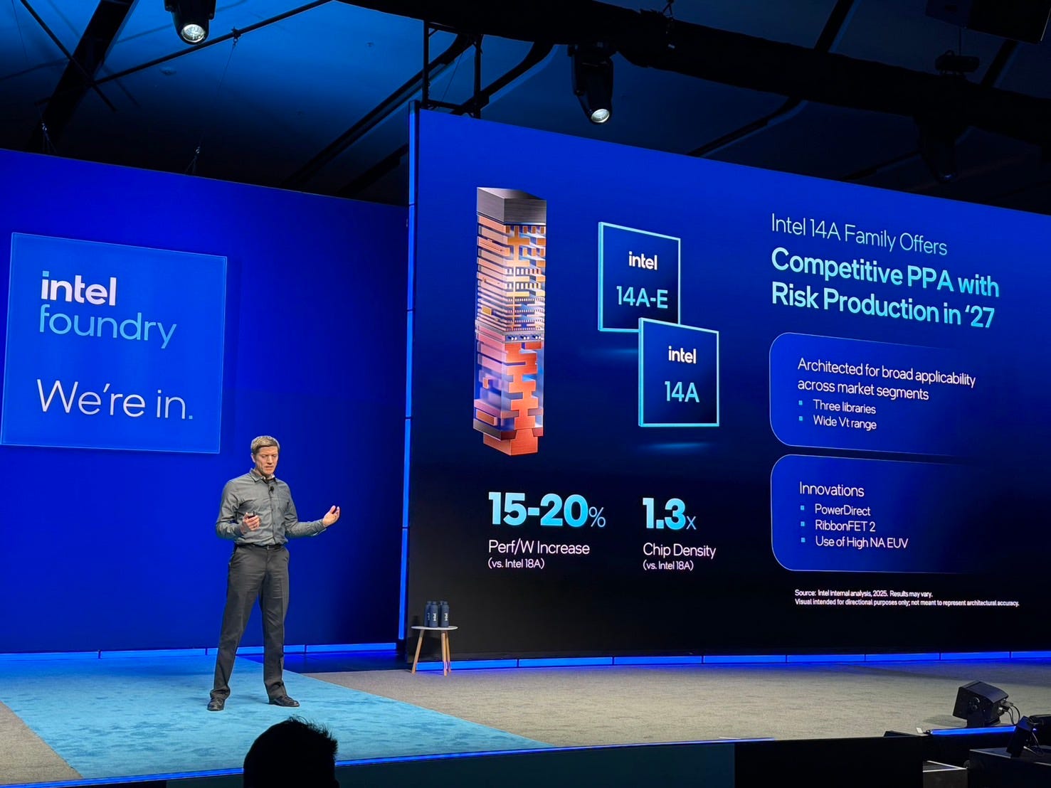
When mapped against TSMC’s process roadmap, Intel’s 14A can be considered a counterpart to TSMC’s A14 node, though there are several key differences between the two:
TSMC A14 (an enhanced 2nm-class node) currently does not adopt backside power delivery via SPR (Super Power Rail). However, TSMC has not ruled out the possibility of introducing SPR in a later version, such as A14P.
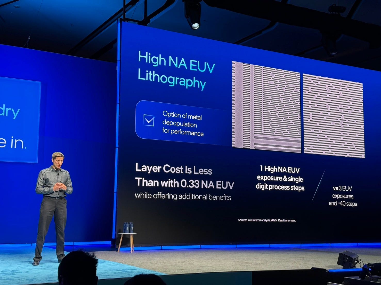
TSMC has publicly stated that even at the A14P node, it has no immediate plans to adopt High-NA EUV lithography, primarily due to cost concerns and manufacturing complexity. As a result, TSMC must develop stricter design rules for A14P to overcome physical limitations without relying on High-NA EUV.
This approach reflects TSMC’s more conservative stance on technology adoption, favoring design-rule-based innovation to navigate scaling challenges—allowing it to retain cost-efficiency and production flexibility at advanced nodes.
Intel and UMC’s Logic Process Collaboration: A 12nm Alliance Model
Another noteworthy development in the market is the process collaboration between Intel and UMC (United Microelectronics Corporation). Intel announced a joint development effort with UMC at the 12nm node, marking a significant step in expanding Intel’s foundry presence into Asia’s mature process segment.
This collaboration structure can be interpreted as follows:

UMC brings customer access and chip design integration, managing frontend market relationships and demand-side logistics.
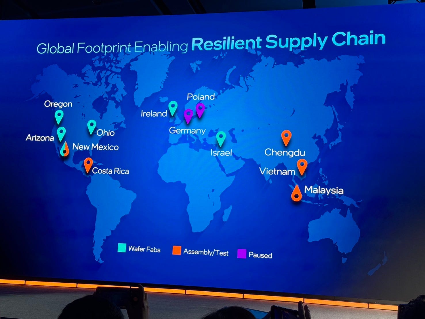
Intel contributes advanced manufacturing capabilities and platform technology, with a focus on domestic U.S. fabs, such as its Arizona facility.
The two parties will adopt a revenue-sharing model, distributing profits based on manufacturing output and customer engagement.

This alliance not only reinforces Intel Foundry Services (IFS) as a global manufacturing platform, but also accelerates Intel’s fab utilization rates and strategic re-engagement with the Asian market.

Key Bottlenecks in Advanced Nodes: Intel 18A’s Capacity and Yield Challenges
For any advanced-node foundry entrant, capacity and yield are the two most critical indicators of competitiveness and customer trust. This is especially true for Intel, following its transition into Intel Foundry Services (IFS).
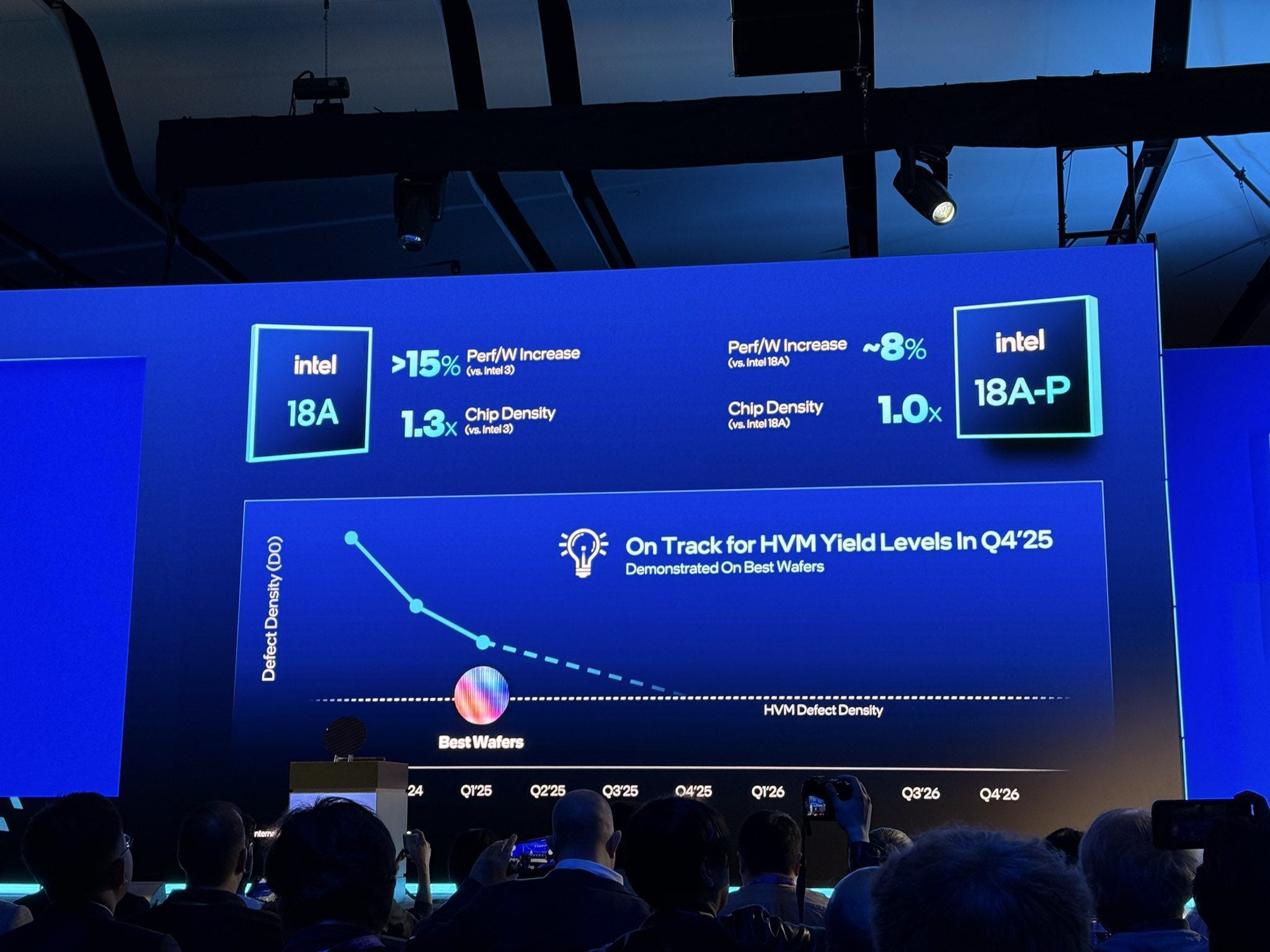
According to research by SemiVision and supply chain observations, while Intel’s flagship 18A process (featuring PowerVia + RibbonFET) has technically entered the initial production phase, its usable capacity remains limited. The main constraints include:
Yield ramp-up not yet stabilized: Due to the introduction of several novel technologies—such as backside power delivery and GAA transistors—the early manufacturing stages face significant challenges with defect density and process stability.

Insufficient maturity of tools and process integration: This includes issues with EUV exposure yields, materials supply chains, and packaging compatibility, all of which are still under optimization.
Customer base concentrated in Tier-1 and Tier-2 segments: Intel’s current 18A customers are primarily high-tier players, likely including hyperscalers, automotive processor makers, and AI chip developers. The process has not yet scaled to the broader mid- and long-tail markets.

This situation suggests that Intel is prioritizing its limited 18A capacity for strategically significant customers, while internally pushing to accelerate yield engineering and move up the manufacturing learning curve—a crucial step in building trust and credibility under the IFS brand.


For any advanced-node foundry entrant, capacity and yield are fundamental indicators of competitiveness and trustworthiness—this is especially true in the case of Intel’s transformation into Intel Foundry Services (IFS).
According to investigations by SemiVision and insights from the supply chain, while Intel’s flagship 18A process (incorporating PowerVia and RibbonFET) has technically reached an early stage of production, its effective usable capacity remains limited. The key bottlenecks are as follows:
Yield ramp-up remains incomplete: The 18A process introduces a range of novel technologies—such as backside power delivery and GAA transistors—which pose significant challenges in terms of defect density and manufacturing stability during the initial production phase.
Tool and process maturity is still lacking: Critical components such as EUV exposure yields, materials supply chains, and packaging process integration are all undergoing continuous refinement.

Customer base remains concentrated in Tier-1 and Tier-2 segments: The current 18A client base largely consists of top-tier players—presumably including hyperscale cloud providers (CSPs), automotive processor vendors, and AI chip developers—with limited penetration into the broader mid- and long-tail markets.
This indicates that Intel is allocating its limited 18A capacity to the most strategically critical customers, while simultaneously investing internally to advance yield engineering and accelerate the manufacturing learning curve—a crucial effort for establishing credibility and trust under the IFS brand.

Toward a Platform Mindset: Intel’s Silicon Platform Ecosystem Blueprint
Looking ahead, Intel is not merely competing at the level of individual process nodes—it is actively building a comprehensive “Silicon Platform Ecosystem” that spans design, manufacturing, packaging, and validation. The current technology roadmap includes:

Intel 18A-P / 18A-PT: Continued evolution and optimization of the GAA node, with multiple variants tailored for distinct applications (e.g., high-performance computing vs. mobile SoCs).
Intel 14A / 14AE: Positioned as the next-generation mainstream logic node, expected to introduce higher-density design rules and broader modular IP support.
Intel 12nm with UMC: A collaborative foundry platform targeting mid-range and mature nodes, developed jointly with UMC to expand IFS’s reach and operational flexibility in the global foundry market.
In essence, Intel is no longer positioning itself solely as a wafer manufacturing provider, but is aiming to build an IFS Ecosystem—conceptually akin to TSMC’s Open Innovation Platform (OIP)—by integrating:
Standardized IP module support
Multi-node process offerings
Advanced packaging technologies (e.g., EMIB, Foveros)
Design enablement services
Co-optimization with customers
When discussing Intel’s transformation and strategic positioning, one fundamental perspective stands out: Intel is both a chip design house and a foundry. This dual identity gives it a unique standing in the semiconductor industry.
Intel Is the First Customer of Its Own Foundry
With a strong in-house design team, Intel has the unique ability to manufacture its own chip designs through its internal foundry—Intel Foundry Services (IFS). This model stands in contrast to pure-play fabless companies like NVIDIA or AMD, as Intel possesses a fully vertically integrated capability.
At the same time, Intel also outsources certain designs to third-party foundries based on product requirements and the maturity of process nodes. In particular, when its own advanced nodes are not fully ramped or have limited capacity, Intel acts as a TSMC customer. For instance, several of Intel’s advanced packaging solutions and GPU-related chips are being fabricated using TSMC’s N5 or N3 process nodes.

This highlights Intel’s dual-track strategy of “Design + Foundry”—leveraging its internal manufacturing to drive technology leadership while maintaining the flexibility to utilize external supply chains when needed.
Microsoft: One of Intel’s Key Strategic Customers
Among Intel’s foundry customers, Microsoft stands out as a critical Tier-1 partner. Their collaboration spans not only the development of data center processors and AI accelerators, but also the co-planning of semiconductor platforms deeply integrated with Azure infrastructure.
The presence of such a "system-level mega-customer" not only enhances the market credibility of Intel Foundry, but also provides valuable real-world validation and deployment scenarios for Intel’s technology roadmap. This plays a positive role in accelerating yield ramp-up and driving platform-level optimization.

Key Highlights of the Collaboration
A Foundry Agreement Worth Over $15 Billion:
In 2024, Microsoft signed a foundry agreement with Intel valued at over $15 billion, commissioning Intel to manufacture Microsoft's custom-designed chips using its advanced 18A process technology. While specific applications have not been disclosed, industry observers widely believe these chips will be used for AI accelerators and data center processors, further enhancing the performance and efficiency of Azure infrastructure.
Deeply Integrated System-Level Collaboration:
Microsoft is not only a foundry customer but also a key partner in Intel’s "system-level foundry" strategy. At the Intel Foundry Direct Connect event in April 2025, executives from both companies showcased their joint achievements in advanced packaging, 3D stacking (Foveros Direct), and chip design, underscoring the depth of platform-level integration between the two.
Azure-Intel Cloud Collaboration:
Microsoft Azure is a founding member of the Intel Foundry Services Cloud Alliance. Together, the two companies are working to optimize cloud-based EDA tools and co-develop secure semiconductor design platforms that support a broad range of applications—from commercial to defense sectors.
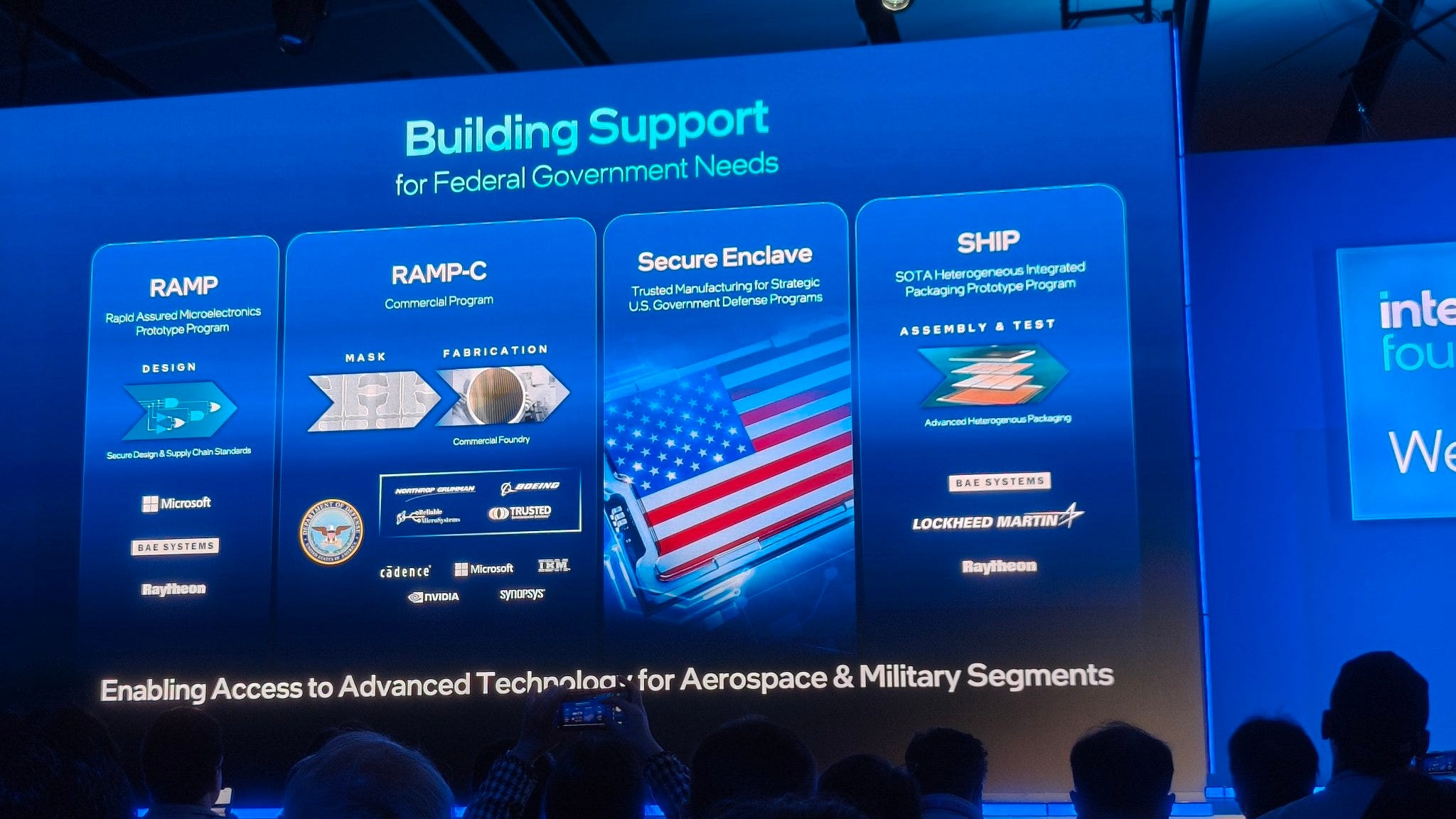
Geopolitically Driven Role in “Manufacturing Sovereignty”
As geopolitical risks have intensified, the U.S. government—starting from the Trump administration—has clearly positioned semiconductor localization and manufacturing sovereignty as strategic imperatives. Among the few companies in the U.S. that still retain advanced logic manufacturing capabilities, Intel has been entrusted with the role of leading this industrial revival.
This strategic role explains why Intel has pursued an aggressive technology roadmap, adopting bold innovations such as PowerVia and RibbonFET in an attempt to regain technological leadership from TSMC. However, semiconductor manufacturing is a long-term game of economic scaling and process maturity—areas where Intel continues to lag behind in terms of yield and volume production.
From a strategic standpoint, though, Intel benefits from strong government support, sustained investor confidence, capital resources, and internal design capabilities. With time and accumulated experience, Intel is expected to gradually close the manufacturing capability gap with TSMC.
In the field of advanced packaging, while TSMC leads with its 3DFabric platform, Intel has also demonstrated significant technological strength. Through a range of innovative packaging technologies, Intel is pushing the boundaries of chip performance and system-level integration. Below is an overview of Intel’s advanced packaging technologies:
For Paid Members , SemiVision will discuss topics on
Overview of Intel’s Advanced Packaging Technologies
Foveros: 3D Stacking Packaging Technology
EMIB: Embedded Multi-die Interconnect Bridge
Co-EMIB: Hybrid Packaging with Foveros + EMIB
PowerVia: Backside Power Delivery
Divergence in Packaging Logic: Intel EMIB vs. TSMC CoWoS-L
Intel: Evolving Toward 12x Reticle EMIB
Intel Advanced Packaging Panorama: From EMIB to Foveros Direct — Defining the Future of Heterogeneous Integration
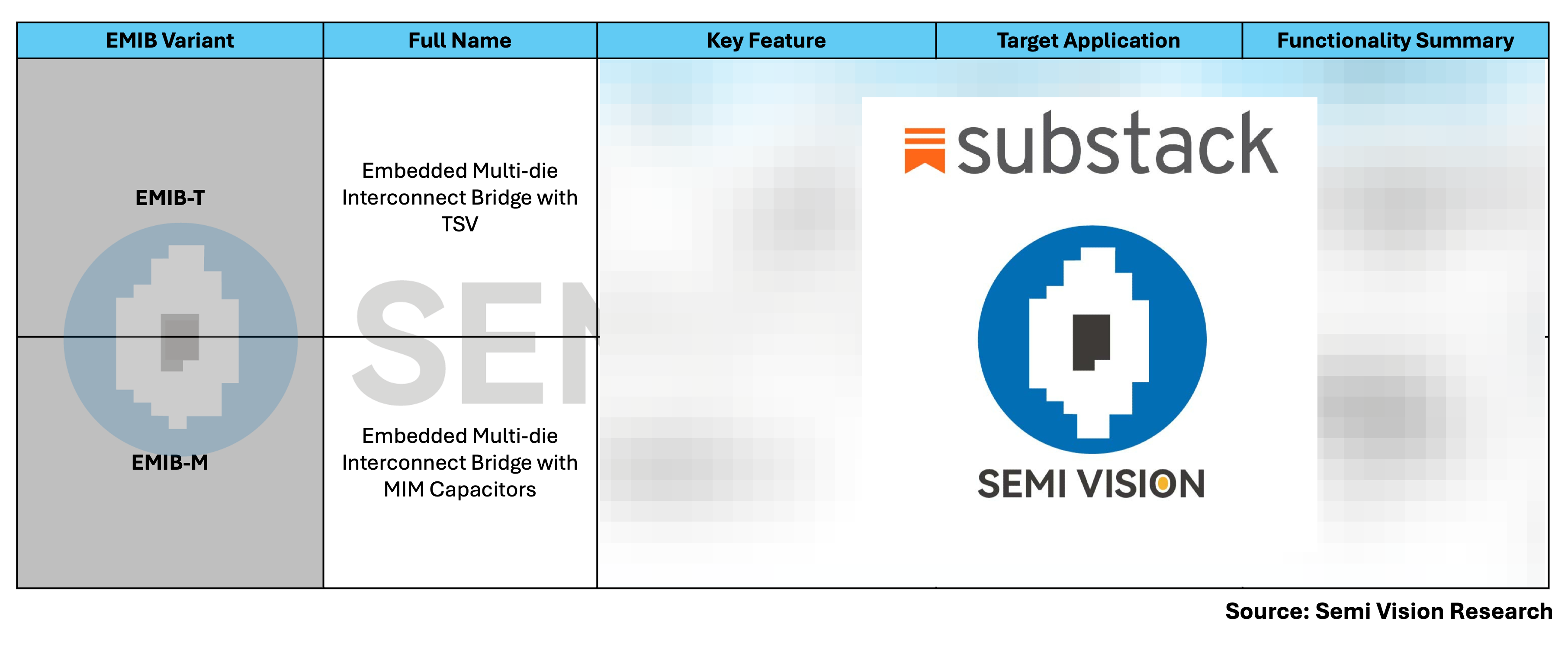
EMIB Family Overview: Intel’s Scalable 2.5D to 3.5D Packaging for Heterogeneous Integration
Foveros Series: A 2.5D/3D Platform for Vertical Stacking and Functional Disaggregation
Innovation Package Key Highlights
Intel’s System Transformation through the Lens of Packaging Platforms
Intel’s CPO + Advanced Packaging Strategy: From Electrical IO to 3D Photonics Integration
Intel OCI Tile Architecture: A Practical Realization of the CPO Roadmap and Modular Integration Strategy
From Architecture to Platform: OCI Tile as a Manifestation of Intel’s CPO Strategy