Foxconn Research Institute:SiliconPhotonic Viewpoint_Optical Interconnection by MicroLED(C2C)
Original Article by SemiVision Research (Foxconn, Nvidia ,Avicena LightBundle)

At this year’s #OFC25 conference and in recent discussions on optical interconnect technologies, optimizing the power efficiency, bandwidth, and transmission range of short-reach interconnects within data centers has become a core topic, driving the emergence of several innovative architectures. Among these, microLED-based optical interconnects have drawn significant attention. MicroLEDs are micron-scale gallium nitride (GaN) light-emitting diodes capable of efficiently emitting photons under electrical current. Unlike traditional VCSELs or external laser sources, microLEDs act as self-emissive microscale light sources, offering a simplified structure, low energy consumption, and full compatibility with CMOS manufacturing platforms—making them ideal for building high-channel-count, massively parallel optical interconnect systems.
Current microLED-based links typically consist of a pair of transceiver chips, integrating a microLED emitter array, a photodiode (PD) receiver array, and driving circuits, connected via multi-core fibers or spatially mapped coherent fiber bundles. Each optical channel is transmitted through an independent core, preserving spatial alignment so the optical emission pattern at the transmitter can be directly mapped onto the PD array at the receiver—enabling what is effectively “optical image transmission.” This architecture aligns exceptionally well with existing chiplet-to-chiplet interconnect standards such as UCIe and BoW. When integrated into large ASIC packages, these microLED transceivers effectively act as an on-package bus extension at the rack level, enabling communication between boards or racks with performance close to in-package signaling, while eliminating the need for traditional SerDes and clock recovery circuits. Prototypes have already demonstrated per-channel speeds of ~10 Gbps, with 128 channels delivering aggregate bandwidths around 1 Tbps. Next-generation systems target 20–25 Gbps per channel, and notably, they use basic NRZ modulation, avoiding the complexity and power overhead of PAM4 or coherent modulation—achieving ultra-low energy consumption at around 2 pJ/bit. Unlike CPO (Co-Packaged Optics), which relies on PIC processes and external lasers, microLED-based interconnects can be fully manufactured on CMOS platforms without exotic materials or precision packaging steps, offering higher process compatibility and potential cost advantages. With a reach of up to 30 meters, significantly exceeding copper cable capabilities, and far greater bandwidth density, microLED interconnects are highly suitable for high-throughput AI/HPC workloads such as GPU-to-GPU or CPU-to-memory connections within and across racks. Of course, challenges remain—packaging integration, yield, reliability, maintainability, and standardization must be addressed. However, as the microLED display industry matures and its supply chain scales, unit costs are expected to drop and may even fall below those of today’s mainstream optical modules. Simple, efficient, and CMOS-compatible, microLED-based optical interconnects could become one of the most disruptive short-reach communication options in future AI/HPC system packaging. As noted in our earlier articles, both academia and industry are investing heavily in this field.
At the Silicon Photonics Forum, Foxconn Research Institute highlighted the concept of using microLED arrays for chip-to-chip optical communication and emphasized the technology’s potential for flexible integration with packaging platforms. Professors at National Yang Ming Chiao Tung University have also conducted long-term research on high-speed optoelectronic components and array-level packaging, exploring system-level optimizations of microLED interconnects for short-reach data center applications. Our team at SemiVision Research continues to monitor the progress of microLED optical interconnect technologies, including materials, chip designs, and ecosystem developments. If you’re interested in further technical details or emerging application insights, feel free to reach out—we’re happy to provide expert analysis and in-depth discussion.
Foxconn Research Institute:SiliconPhotonic Viewpoint _Opportunity and Challenges


For Paid Members, SemiVision will discuss topics on
microLED Optical Interconnects: Current Landscape and Future Potential
Existing Prototypes and Solutions for microLED Optical Interconnects
Leading Companies and Research Institutions Driving microLED Optical Interconnect Development
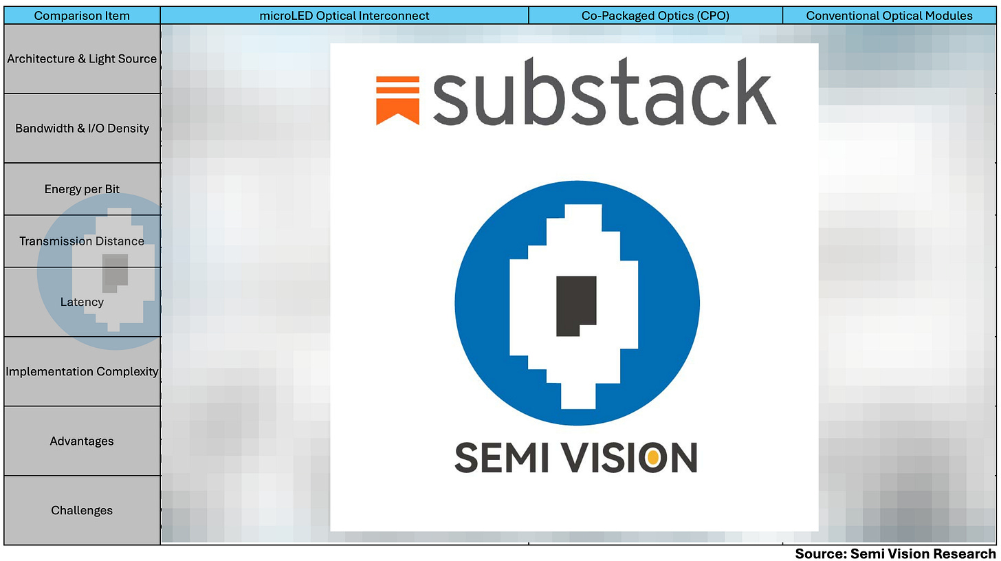
Comparison of microLED Optical Interconnects with CPO and Conventional Optical Modules
Compatibility and Integration of microLED Optical Interconnects with UCIe/BoW Chiplet Interfaces
Future Trends and Potential of microLED Optical Interconnects