


Foxconn Research Institute:SiliconPhotonic Viewpoint _Opportunity and Challenges
Original Article by SemiVision Research

The Foxconn Research Institute has provided strategic insights into the silicon photonics industry, underscoring its critical role in meeting the rising demands of high-performance computing (HPC) and artificial intelligence (AI) applications. The institute identifies silicon photonics as a foundational technology for overcoming bandwidth bottlenecks and enhancing energy efficiency within modern data centers. To advance its competitiveness in optical communication and interconnect solutions, Foxconn Research Institute is actively investing in research and development aimed at integrating silicon photonics into Foxconn’s broader manufacturing ecosystem. This initiative not only supports Foxconn’s long-term innovation strategy but also aligns with the global momentum toward adopting silicon photonics to address the performance and scalability needs of next-generation computing architectures.
The Hon Hai Research Institute (HHRI) represents a key step in Foxconn Group’s development strategy towards our F3.0 transformation to new industries goal. HHRI focuses on prospective technologies over the next 3–7 years, thereby strengthening the Group’s technological and product innovations, supporting enhancements in core competitiveness.


Foxconn 3+3 strategy:
3 key industries: electric vehicles, digital health, and robotics.
3 key technologies: AI, semiconductors, and next-generation communications.

Foxconn’s Full-Stack AI Strategy: Vertical Integration from H100 Modules to Data Centers
As generative AI fuels a new wave of computing, global tech giants are accelerating their investments in AI infrastructure. Foxconn Technology Group is strategically positioning itself as a vertically integrated player, spanning the entire stack from chips to servers and data centers. Based on the latest presentation materials, it is evident that Foxconn is evolving beyond its traditional role as the world’s largest electronics manufacturing service provider to become a key system integrator in the AI supply chain.
The solution stack begins with NVIDIA H100 GPU modules, which are assembled into high-density acceleration units through Foxconn’s in-house developed GPU sub-systems. These are then integrated into Generative AI servers housing eight H100 GPUs—purpose-built for training and inference workloads of large language models (LLMs) such as ChatGPT, Gemini, and Claude. At this level, Foxconn has already demonstrated the ability to produce a full AI server product line that can compete alongside leading HPC providers.
For paid members , SemiVision Research will discuss the topics on
Silicon Photonics Ecosystem (TSMC , Nvidia ,Taiwan SiliconPhotonic)
The Evolution of Optoelectronic Interconnects
How TSMC and Foxconn Are Redefining AI Interconnect Efficiency
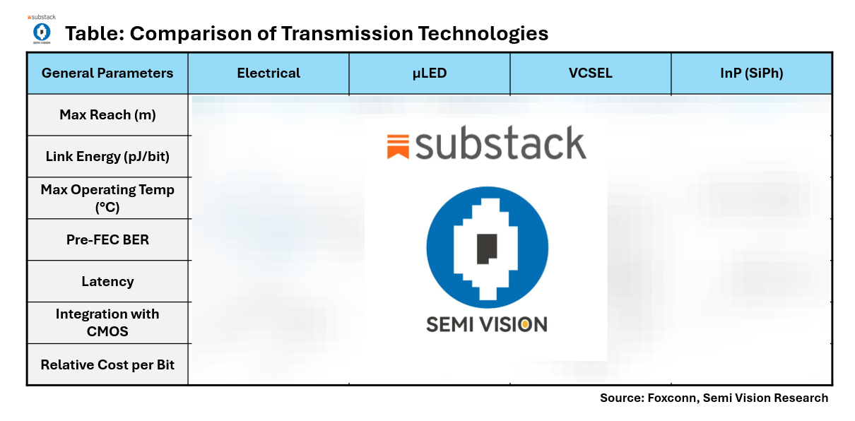
Table: Comparison of Transmission Technologies
Table: Optical Transceiver Evolution
A Full-Distance Efficiency Map for AI-Era Interconnect Technologies

If you would like to explore the silicon photonics roadmaps of TSMC and NVIDIA in greater depth, please refer to our previously published articles for more detailed analysis and insights.
How TSMC’s Silicon Photonics Could Impact NVIDIA’s Future
2025 GTC Review: The Silicon Photonics Era Has Arrived – Get Ready!
NVIDIA x TSMC: A Milestone in Silicon Photonics and Optical Integration
Nvidia GTC AI Conference Preview: GB300, CPO switches, and NVL288
TSMC and NVIDIA Pioneering the Future of AI with Silicon Photonics Technology
CPO Switch Technology Analysis
How to Distinguish Between CPO and OIO? What Is Their Fundamental Difference?
How TSMC’s Silicon Photonics Could Impact NVIDIA’s Future
UMC’s Strength in the Silicon Photonics Supply Chain
Silicon Photonics Supply Chain – Opportunities and Challenges for Taiwan’s Supply Chain