Intel Showcases Groundbreaking Innovations at IEDM 2024
Advancing Heterogeneous Integration, GAA Transistors, and Ruthenium Interconnects for the Next Era of Semiconductor Technology

At IEDM 2024, Intel plans to deliver two invited talks and present seven research papers. During a pre-event briefing for the press, Sanjay Natarajan, Senior Vice President and General Manager of Intel's Technology Research Group, previewed some of the innovations Intel plans to showcase.
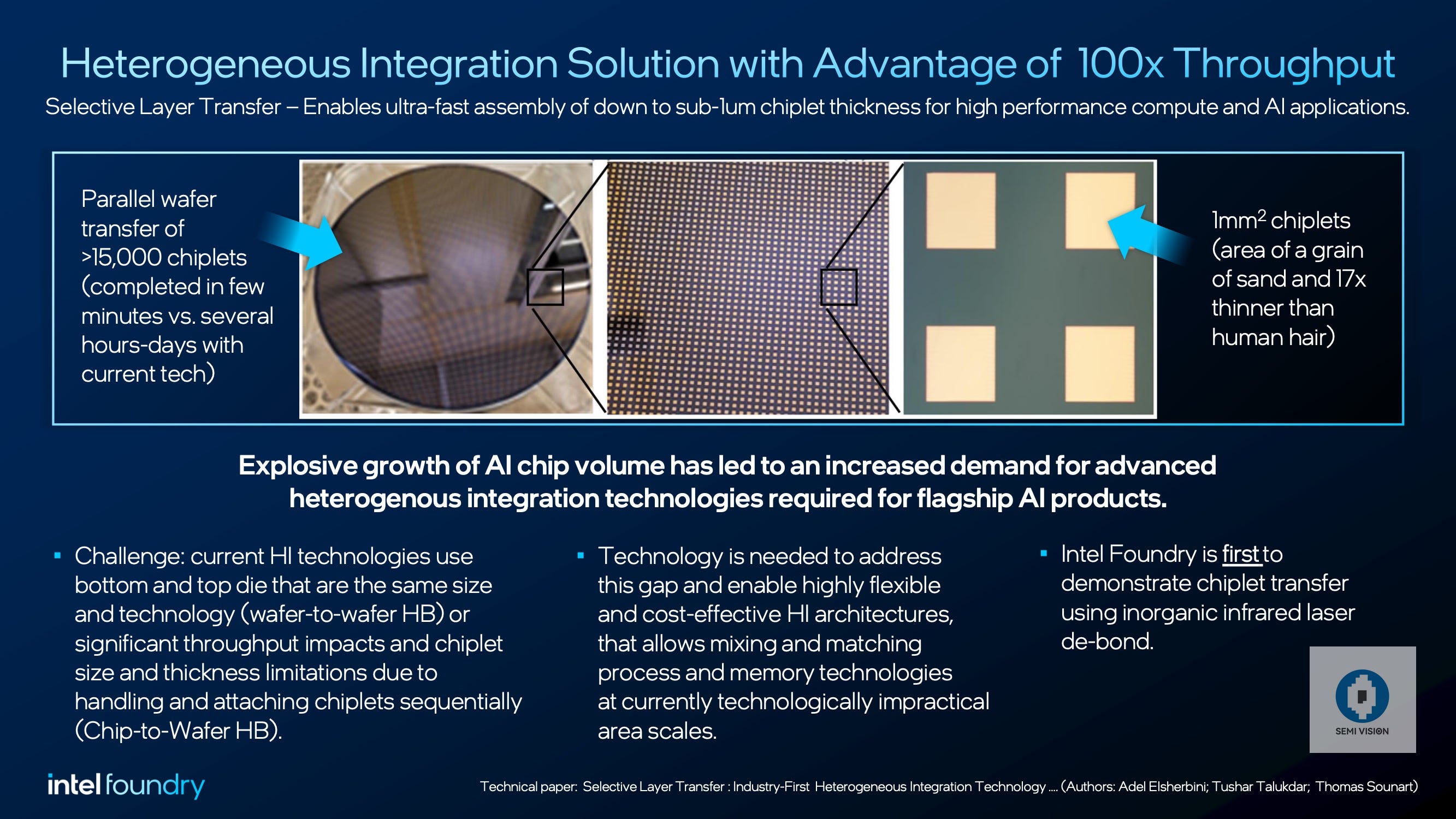
Heterogeneous Integration (HI)
Intel highlighted advancements in HI, a technique enabling the combination of various chiplets tailored for specific functions into a single product. This trend allows for greater flexibility in CPU designs, such as Lunar Lake, and is pivotal for next-generation computing.
Traditionally, HI chiplets were produced using two methods:
Wafer-to-Wafer (W2W): Bonding two dies of the same size and technology at the wafer level, which is cost-effective.
Chip-to-Wafer (C2W): Placing chiplets onto a separate wafer, which is more expensive and time-consuming.

Intel introduced a breakthrough by utilizing inorganic infrared lasers to debond over 15,000 chiplets (each measuring 1 mm²) from a single wafer within minutes. They emphasized the importance of modularity in future chiplet stacking technologies and announced developments in next-generation EMIB.
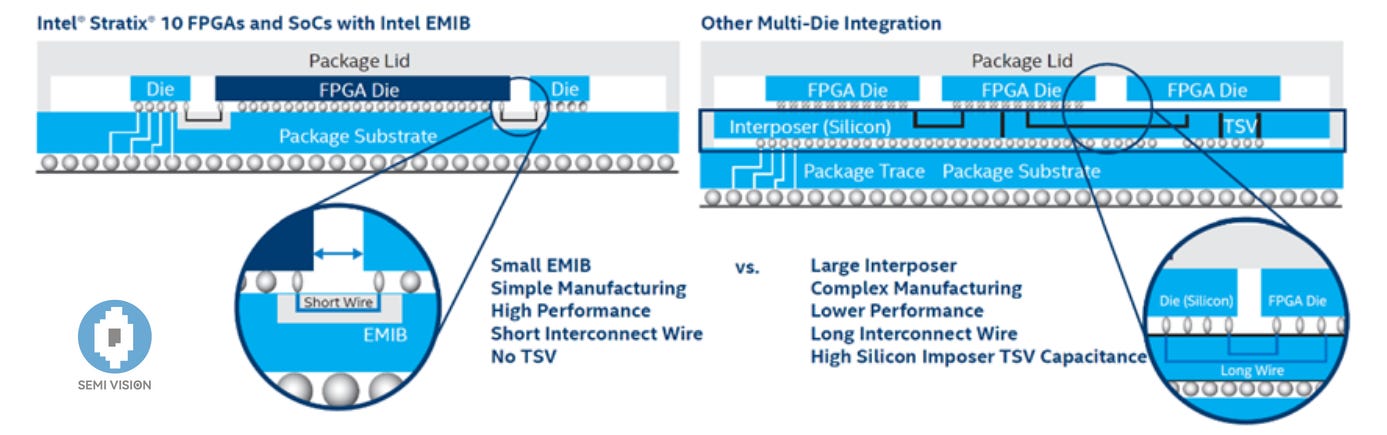
EMIB (Embedded Multi-die Interconnect Bridge)
The original concept of silicon bridge invention likely did not originate from Intel. TSMC also had related invention concepts in the early days. However, Intel refined the silicon bridge and applied it to 2.5D packaging, achieving not only excellent computational performance and low power consumption but also cost savings. Intel has effectively carved out its own path in advanced packaging technology using EMIB, avoiding direct competition with TSMC's CoWoS technology.
Compared to other multi-die integration packaging technologies, Intel emphasizes the advantages of its EMIB technology:
EMIB is compact, resulting in shorter signal transmission paths between dies.
It does not require through-silicon vias (TSVs) or interposers, simplifying the manufacturing process.
It enhances computational performance.

Additionally, improvements in GAA performance were demonstrated by covering molybdenum disulfide (MoS₂) electrodes with hafnium oxide (HfO₂), achieving subthreshold swing improvements (75 mV/d or better). This advancement reinforces the possibility of sustaining Moore's Law with GAA technology, a topic expected to be explored in one of Intel's invited talks.
Additionally, improvements in GAA performance were demonstrated by covering molybdenum disulfide (MoS₂) electrodes with hafnium oxide (HfO₂), achieving subthreshold swing improvements (75 mV/d or better). This advancement reinforces the possibility of sustaining Moore's Law with GAA technology, a topic expected to be explored in one of Intel's invited talks.
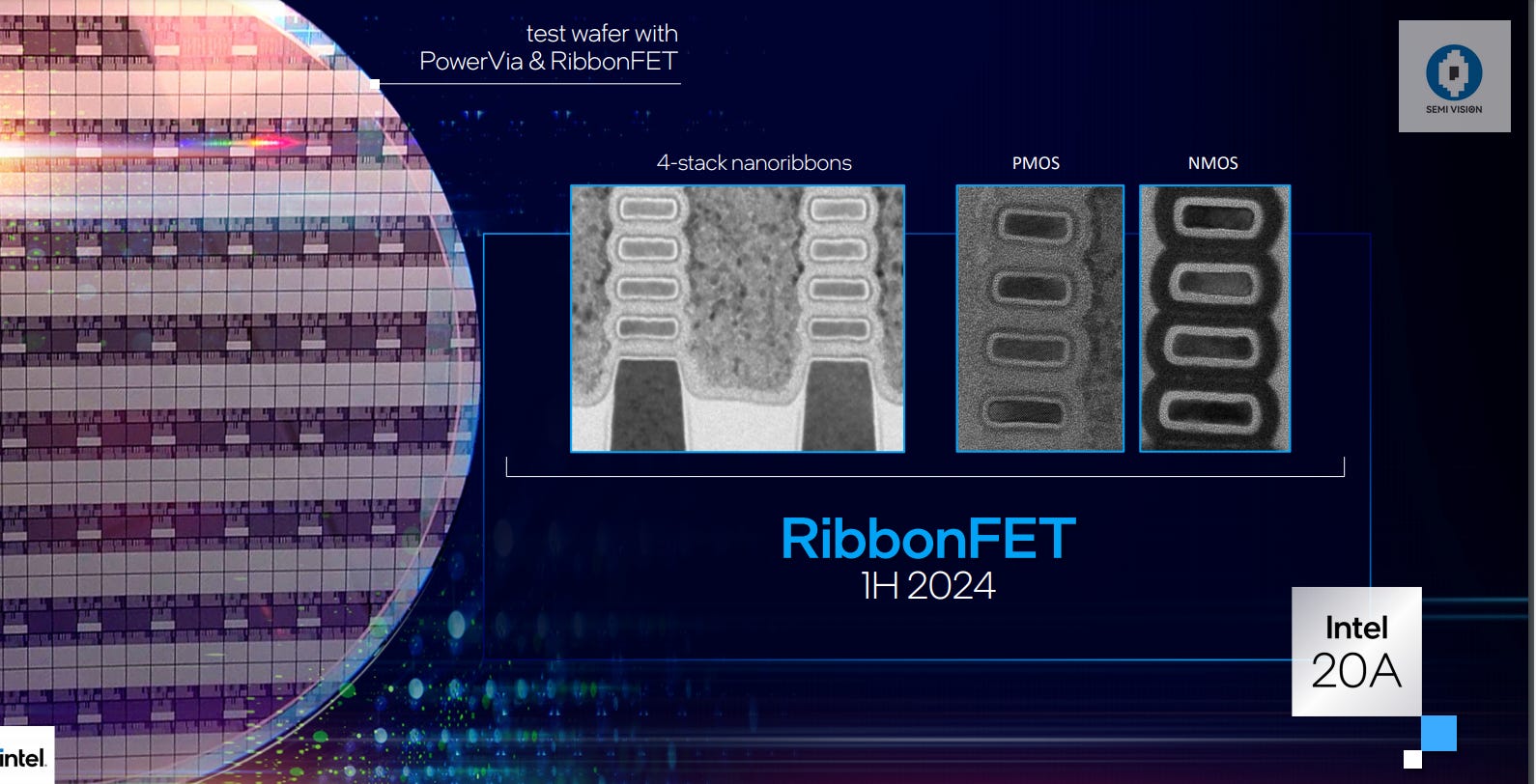
Transistor Innovations
Intel also shared updates on its RibbonFET, a Gate-All-Around (GAA) transistor design, used in Intel 20A, 18A, and 14A nodes. Intel has prototyped highly efficient transistors with a gate length of 6 nm and a fin thickness of 1.7 nm.