

Lightmatter at Computex 2026: The AI Infrastructure Bottleneck Has Shifted from Compute to Interconnect
Original Article By SemiVision Research [Reading time: 12 mins]

Lightmatter at Computex 2026: The Next Bottleneck in AI Infrastructure Is No Longer Compute — It Is Interconnect
At Computex 2026, Lightmatter founder and CEO Nick Harris delivered a message that is becoming increasingly difficult for the AI infrastructure industry to ignore: the next major bottleneck in AI is no longer raw compute. It is interconnect.
This may sound like a photonics company making the case for photonics, but the structural logic is much deeper. Over the past decade, the semiconductor industry has focused on bigger GPUs, more advanced process nodes, higher HBM bandwidth, and larger AI clusters. But as models move into the trillion-parameter era, and as Mixture-of-Experts architectures, long-context inference, prefill/decode separation, and multi-rack training become mainstream, the central challenge is no longer whether a single accelerator is fast enough.
The real question is whether thousands — eventually tens of thousands — of XPUs can operate as one giant distributed brain.
That is the core of Lightmatter’s argument: AI scaling has become an interconnect problem.
AI Growth Has Outpaced the Power and Network Foundation
AI workloads are growing explosively. Training requires huge amounts of synchronous communication. Inference is increasingly constrained by time-to-first-token, decode latency, memory bandwidth, KV cache movement, and network hop count.
This is especially obvious in MoE models. MoE allows AI models to scale parameter count without activating the full model for every token, but it also creates a much more complex communication pattern. Tokens need to move between experts, accelerators, racks, and memory pools. The more distributed the model becomes, the more the network determines the real system performance.
In other words, the bottleneck is shifting.
Previously, the industry asked: how powerful is the GPU?
Now the more important question is: can data move quickly, efficiently, and predictably to the right accelerator at the right time?
This is why Lightmatter frames optical interconnect not as a replacement for existing optics, but as a new infrastructure layer for AI systems. The value is not simply higher bandwidth. The value is higher GPU utilization, lower latency, lower power per bit, and better system-level scalability.
In the AI factory era, the winning metric will not only be FLOPS. It will be tokens per watt, tokens per second per dollar, and the ability to keep a massive distributed compute system fully utilized.
Training, Prefill, and Decode Are Three Different Bottlenecks
One of the most important points in Lightmatter’s presentation was the separation of AI workloads into three categories:
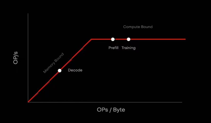
Training, inference prefill, and inference decode.
These workloads may all run on AI accelerators, but they stress infrastructure in very different ways.
Training is dominated by collective communication. Large GPU clusters need to synchronize gradients, exchange intermediate results, and maintain parallel efficiency across many devices. If the network cannot keep up, expensive GPUs sit idle waiting for data.
Inference prefill is dominated by time-to-first-token, or TTFT. For chatbots, enterprise agents, coding assistants, and real-time AI applications, the user experience is strongly shaped by how quickly the first token appears.
Inference decode is different again. Decode is often latency-sensitive, memory-intensive, and highly dependent on KV cache access. As context length increases, decode becomes more constrained by memory movement and interconnect latency.
This is why Lightmatter argues that optical interconnect can improve the entire AI workload curve, not just peak bandwidth. According to the presentation materials, Passage can help reduce training time by around 3 times, reduce TTFT by around 3 times, and improve decode interactivity by around 11 times.
The exact numbers matter, but the bigger message matters more: photonic interconnect is moving from a networking component into a system-level AI performance component.

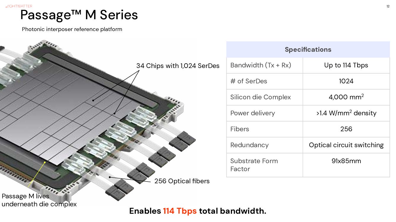
Passage Is Not Just an Optical Module. It Is a Photonic Interposer
Lightmatter’s central platform is Passage. Many people may initially classify it as CPO or an optical module, but that understates the ambition.
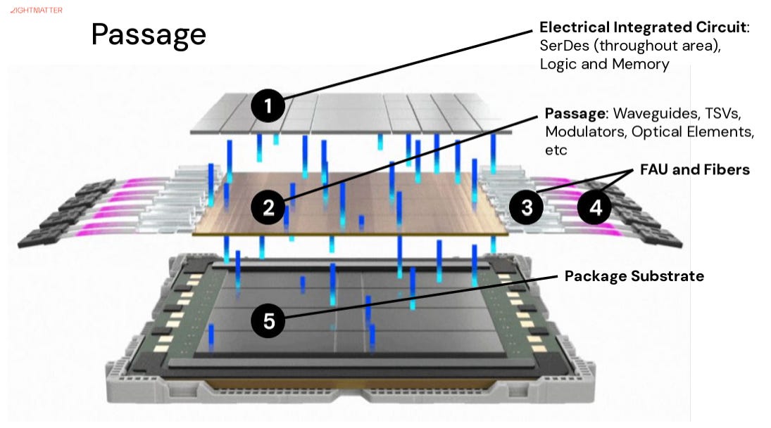
Passage is better understood as a photonic interposer architecture. It brings optics into the package-level and system-level fabric of AI computing.
In traditional architectures, chip I/O is constrained by the edge of the die. This is often described as the shoreline problem. A chip is like an island: all external connections must pass through the coastline. As chips become larger and data movement becomes more intense, the edge becomes a bottleneck.
Passage attempts to break this limitation by moving optical I/O deeper into the package and across the die complex. Instead of relying only on the chip edge, photonic interconnect can be placed much closer to where data is generated and consumed.
This is the key difference between conventional pluggable optics and Lightmatter’s architecture.
Pluggable optics sit outside the system.
CPO brings optics closer to the switch or accelerator.
A photonic interposer makes optics part of the AI compute fabric itself.
That is why Passage M1000 is positioned as a photonic superchip, not merely an optical engine. The product includes 114 Tbps of bandwidth, 1,024 SerDes, a large photonic interposer, built-in optical circuit switching, and a packaging concept designed for high-density AI systems.
The implication is clear: optical interconnect is entering the same strategic layer as advanced packaging, HBM integration, silicon interposers, and AI accelerator architecture.
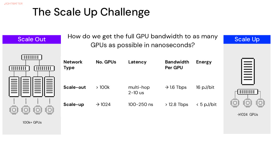
From Scale-Up and Scale-Out to Scale-Across
Lightmatter also divides future AI interconnect into three expansion domains.
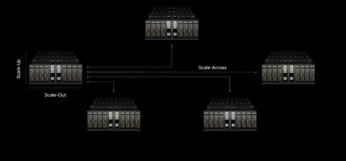
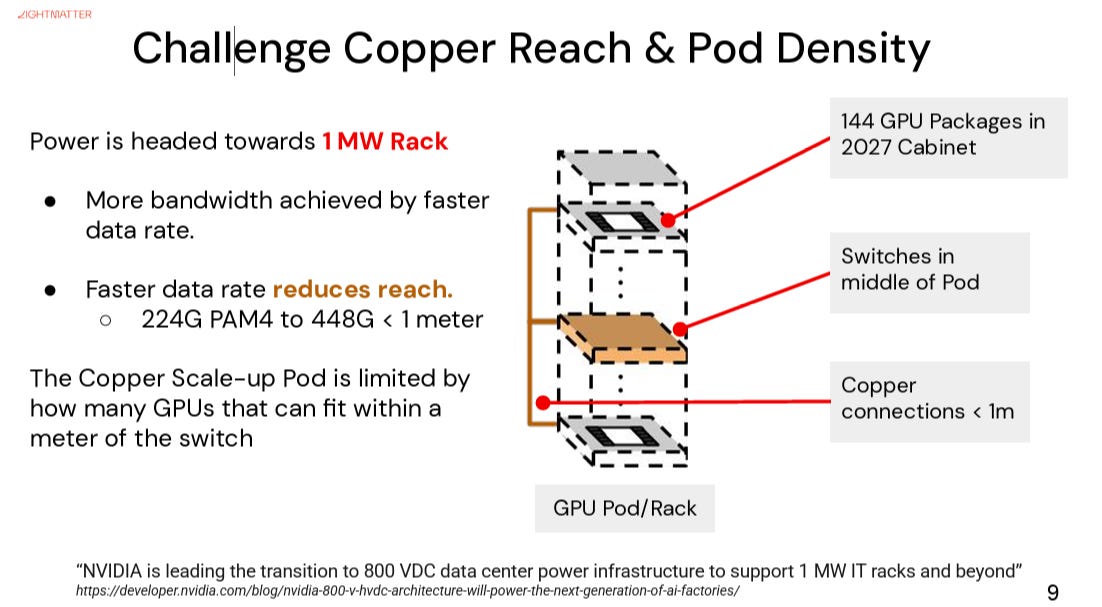
Scale-up refers to short-distance interconnect, usually inside a rack or pod, around the one-meter level.
Scale-out refers to interconnect across racks or rows in the data center, around the 100-meter level.
Scale-across refers to much longer-distance interconnect across data centers or AI campuses, potentially 10 kilometers or more.
Copper still has advantages at very short distances. But as data rates increase, copper faces worsening insertion loss, crosstalk, retimer power, connector complexity, and PCB material constraints. At 224G and beyond, the cost of keeping electrical signaling alive rises sharply.
This is where optics becomes structurally important.
The point is not that optics will replace copper everywhere. The point is that optics will take over the high-bandwidth, high-density, low-latency, and longer-reach portions of the system where copper becomes too power-hungry or too complex.
Future AI infrastructure will likely become a hybrid system: copper remains relevant inside tightly coupled packages and boards, while optics expands from rack-to-rack networking into scale-up domains, CPO, NPO, and eventually photonic interposers.
NPO, CPO, and Photonic Interposer: The Roadmap Is Becoming Clear
Lightmatter’s roadmap reflects three levels of optical integration.
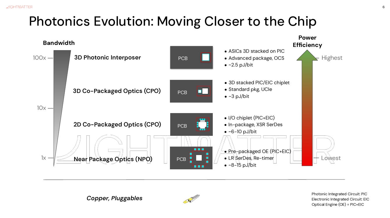
The first level is NPO or optics-near-package. This brings optical connectivity closer to the XPU or switch ASIC, but does not fully embed optics into the package architecture. Passage L20 fits into this direction and is designed as a general optical interconnect product for NPO, CPX, and XPO applications.
The second level is CPO, or co-packaged optics. Here, optics moves much closer to the switch or accelerator silicon. This reduces electrical reach, lowers power, and increases bandwidth density.
The third level is the photonic interposer, represented by Passage M1000. This is the more radical architecture. Optics is not only near the chip. It becomes part of the chiplet and package fabric.
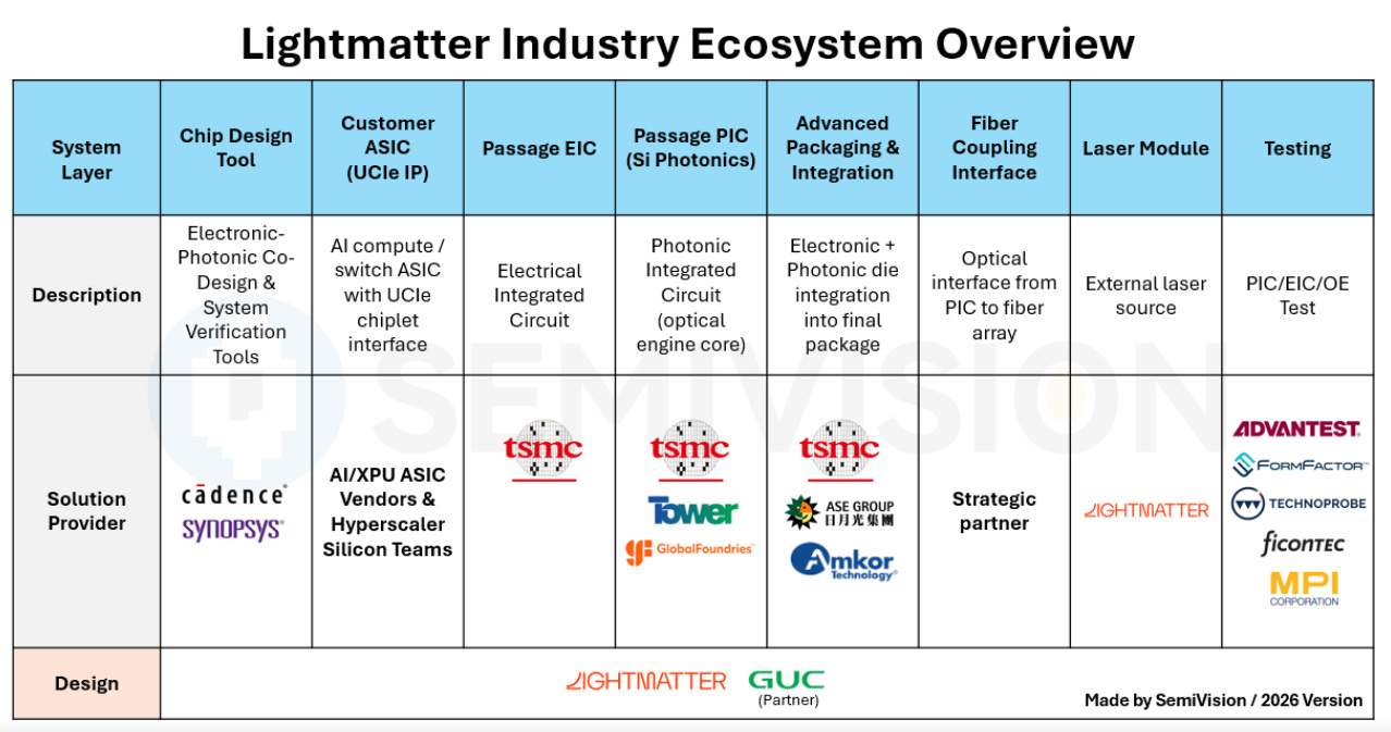
This roadmap is very important for the semiconductor supply chain because it collapses several previously separate industries into one system problem.
Advanced packaging, silicon photonics, SerDes, optical fiber arrays, external laser sources, liquid cooling, OSAT assembly, wafer-level testing, interposer manufacturing, and data center serviceability all become connected.
For Taiwan, this is especially relevant. The island already plays a central role in foundry, advanced packaging, substrates, AI servers, liquid cooling, and system integration. If photonic interposers and CPO move into volume production, Taiwan’s role in AI infrastructure could move even deeper — from assembling AI servers to building the optical nervous system of AI factories.

Guide: Laser Sources Become AI Infrastructure Components
Another important product in Lightmatter’s portfolio is Guide, which the company positions as part of its very large scale photonics strategy.
This matters because if every AI cluster requires massive optical I/O, then laser sources themselves become a bottleneck. Traditional systems rely on many pluggable optics and distributed lasers, but this creates faceplate congestion, thermal complexity, maintenance burden, and many potential failure points.
Guide takes a different approach. It centralizes high-density laser sources into a liquid-cooled laser platform designed to support co-packaged optical systems.
The strategic message is simple: light generation is becoming an infrastructure layer.
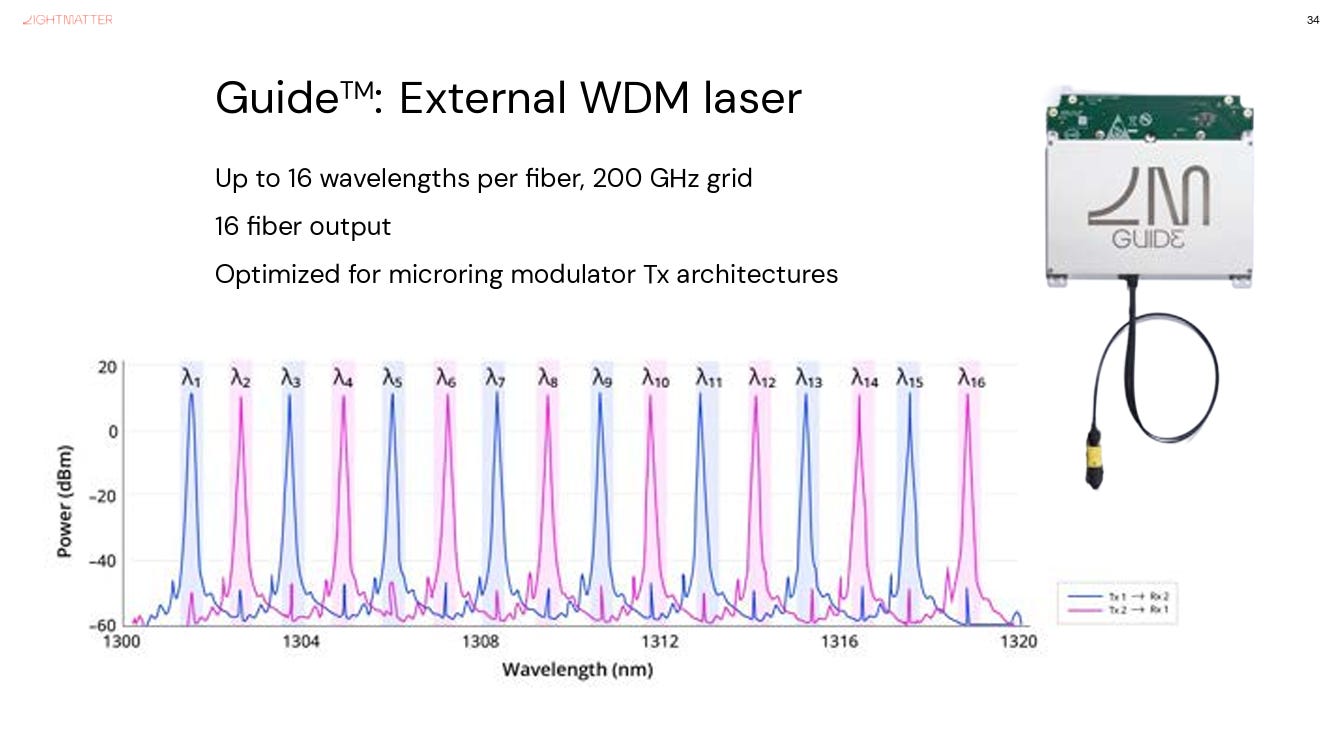
In the past, lasers were treated as components inside optical modules. In the future, high-density external laser sources may become shared resources in AI systems, similar to how power shelves, cooling loops, and switch fabrics are treated as infrastructure.
This shift will create new requirements for thermal design, laser reliability, wavelength stability, optical coupling, field replacement, and system-level monitoring.
For the supply chain, this means that laser packaging, thermal interface materials, precision alignment, micro-optics, liquid cooling, and reliability testing will become more important.

eClick and vClick: Solving the Serviceability Problem of CPO
One of the biggest barriers to CPO adoption has always been serviceability.
Pluggable optics are attractive because they are easy to replace. If a module fails, the operator can remove it and install a new one. But when optics are integrated closer to the ASIC or package, the maintenance model becomes more difficult.
If an optical connection fails, does the whole expensive switch or accelerator package need to be replaced?
This question has limited the pace of CPO deployment.
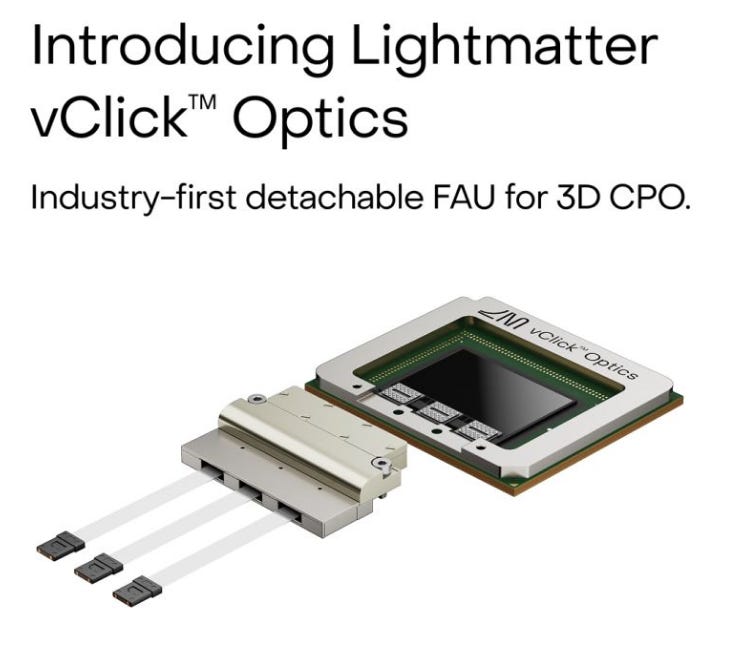
Lightmatter: We has announced vClick™ Optics, the first Advanced Packaging compatible dFAU for high-bandwidth Co-Packaged Optics, ensuring high production yield and field serviceability. This breakthrough includes support for pluggable DWDM fiber with an insertion loss of less than 1.5 dB. We are proud to work with SENKO Advanced Components, Inc. and ASE Global on innovative solutions that enable massively deployable and serviceable Passage 3D photonic interconnects.
Lightmatter’s eClick and vClick are designed to address this issue by providing removable optical fiber array units compatible with advanced packaging. The goal is to preserve the density benefits of co-packaged optics while maintaining a realistic field-service model.
This is a major point. CPO cannot scale only by showing better bandwidth or lower power. It must also prove that hyperscalers can operate, maintain, and repair these systems at data center scale.
In that sense, eClick and vClick are not just connector technologies. They are part of the economic foundation required for CPO deployment.
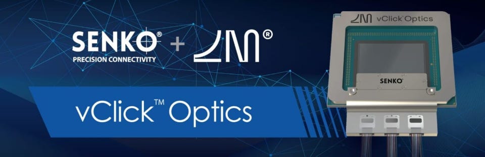
The key advantages of vClick include:
High-bandwidth DWDM compatibility: Supports broadband coarse wavelength division multiplexing (CWDM) and dense wavelength division multiplexing (DWDM) over a wide optical spectrum of up to 80+ nm, enabling large-scale optical bandwidth density and flexibility.
Advanced packaging compatibility: The technology is compatible with mold-and-grind advanced packaging process flows used by major global foundries and outsourced semiconductor assembly and test providers (OSATs).
Automated assembly: No active fiber alignment is required during production, helping reduce assembly and testing time.
Field serviceability: With measured insertion and repeated mating losses below 1.5 dB, vClick can preserve the optical power budget required for field-serviceable CPO systems supporting bandwidths above 100 Tbps.
BiDi and DWDM: Fiber Economy Becomes Data Center Economy
Lightmatter also emphasizes bidirectional optical technology, or BiDi.
At small scale, fiber count may look like a cabling issue. At AI data center scale, it becomes an economic issue.
A 512-XPU or 1,024-XPU system can require enormous numbers of fibers and connectors. Every additional fiber increases installation complexity, service cost, space requirements, and potential failure points.
BiDi allows transmit and receive signals to share optical infrastructure more efficiently. Combined with DWDM, it can reduce fiber count and improve bandwidth density.
This is why the future of AI networking will not be determined only by lane speed. It will also be determined by fiber efficiency, connector reliability, optical alignment, wavelength management, and total installed network cost.
In large AI factories, optical architecture is not just a performance decision. It is a data center economics decision.
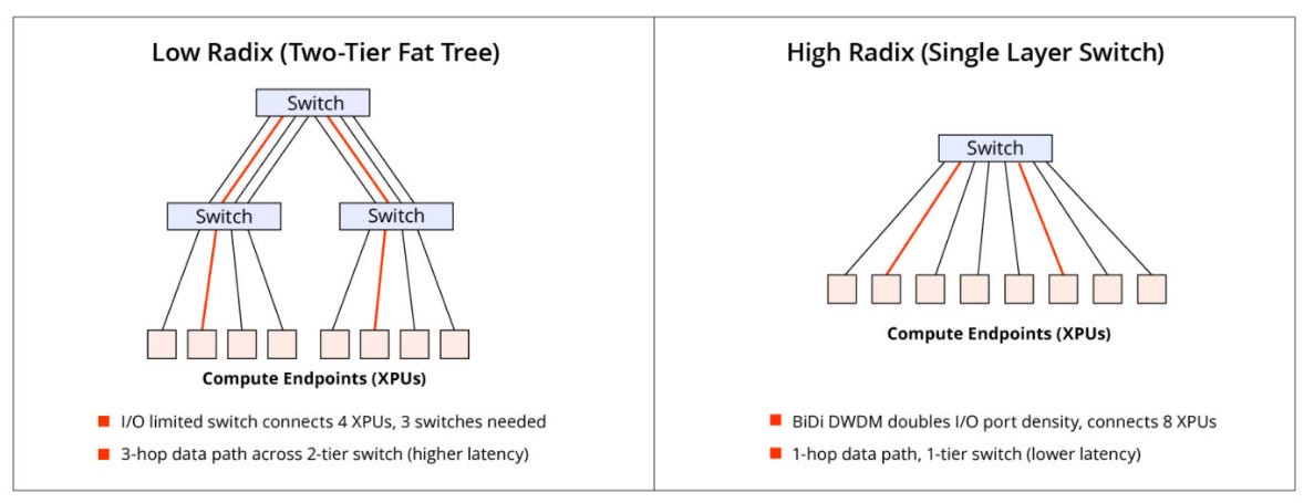
Why Radix Matters: Power, Performance, and Cost Savings
Lightmatter BiDi technology doubles the radix of a network switch without increasing the number of optical fibers in the network. A higher radix, as illustrated above, reduces the number of hops a data packet must take to cross the network. Fewer hops mean fewer switches are needed for a given bisection bandwidth—enabling lower hardware costs and reduced power consumption. Put another way, increased radix (and bandwidth) enables larger, higher performing AI compute clusters without a corresponding increase in the number of switch tiers in their network. A network with fewer switch nodes inherently consumes less power.
Finally, fewer hops translate directly into lower end-to-end latency and greater predictability. For tightly-coupled AI training workloads where GPUs are in constant communication, minimizing this latency is paramount for maximizing the overall computational efficiency. Specifically for Mixture-of-Experts (MoE) models, a higher radix allows expert parallel communications to remain within the high-bandwidth domain, preventing them from being bottlenecked by slower scale-out networks. This enables MoE models with a larger number of experts and finer-grained expert configurations, which are crucial for increasing model capacity and achieving faster training times.
From a SerDes-Centric World to a Photonics-Centric World
For many years, high-speed interconnect has been SerDes-centric. The industry has competed on faster electrical lanes, better equalization, better retimers, lower bit error rate, and stronger signal integrity.
SerDes will remain critical. But the center of gravity is changing.
As data rates continue to rise, relying only on stronger SerDes, more retimers, more complex PCB materials, and higher-end connectors becomes increasingly expensive. At some point, the system has to move the optical boundary closer to the compute boundary.
That is the transition Lightmatter is betting on.
The industry is moving from using optics as a long-distance transport layer to using optics as an architectural layer for AI computing.
This is the real meaning of optical infrastructure.

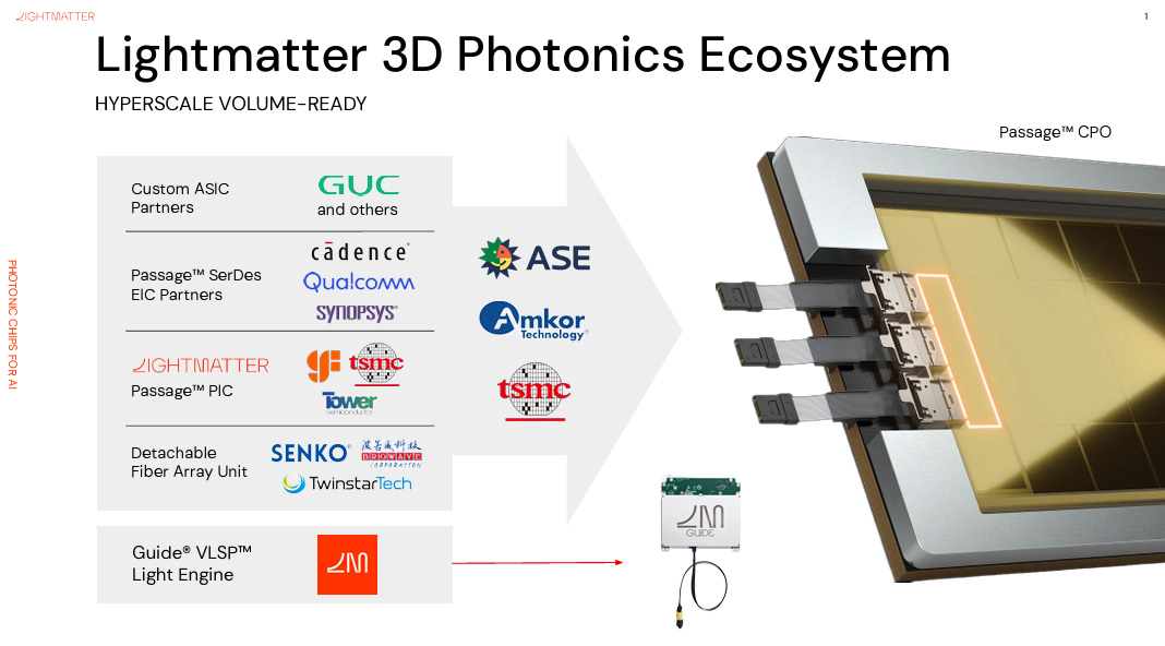
Lightmatter’s 3D photonics ecosystem
For hyperscale AI infrastructure, centered around its Passage™ CPO platform. Rather than positioning Passage as a standalone optical interconnect product, Lightmatter presents it as a full supply-chain ecosystem that combines custom ASIC partners, SerDes electrical IC partners, photonic IC partners, detachable fiber array unit suppliers, and its Guide® VLSP™ light engine. The key message is that scaling AI infrastructure now requires a tightly integrated photonics and advanced packaging platform, where optical connectivity, electrical signaling, packaging, and fiber attach are co-designed for high-volume deployment.
March 11, 2026 - Lightmatter announced a major milestone for AI optical interconnects, demonstrating its Passage™ Co-Packaged Optics chiplet with a record 1.6 Tbps throughput per fiber. The platform uses a 16-wavelength DWDM architecture with 112G SerDes lanes, delivering up to 8x higher bandwidth per fiber than existing NPO and CPO solutions.
By combining Lightmatter’s Passage photonic engine with Qualcomm Technologies’ 112G PAM4 optical SerDes chiplet, the company is positioning its technology as a high-volume-ready CPO architecture for hyperscale AI data centers. The key significance is not only higher bandwidth density, but also lower fiber count, reduced cabling complexity, better power efficiency, and a clearer path toward 100 Tbps and beyond per package for next-generation XPUs and switches.
Conclusion: The Next Foundation of the AI Factory Is Optical
The key message from Lightmatter’s Computex 2026 presentation can be summarized in one sentence:
The next bottleneck in AI is not only compute. It is interconnect. And the next generation of interconnect will increasingly be optical.
From Passage M1000 and photonic interposers, to L20/L200 for NPO and CPO, to Guide laser platforms, BiDi, DWDM, eClick, and vClick, Lightmatter is not building a single component. It is building an optical infrastructure stack for AI factories.
If NVIDIA defines the GPU and rack-scale computing layer of the AI factory, Lightmatter wants to define how data moves inside that factory.
This has major implications for the semiconductor industry.
The future AI data center will not be won only by buying more GPUs. It will be won by connecting those GPUs into a more efficient, lower-latency, lower-power, and more scalable system.
In that system, photonics is no longer just a supporting technology.
It is becoming the nervous system of AI infrastructure.
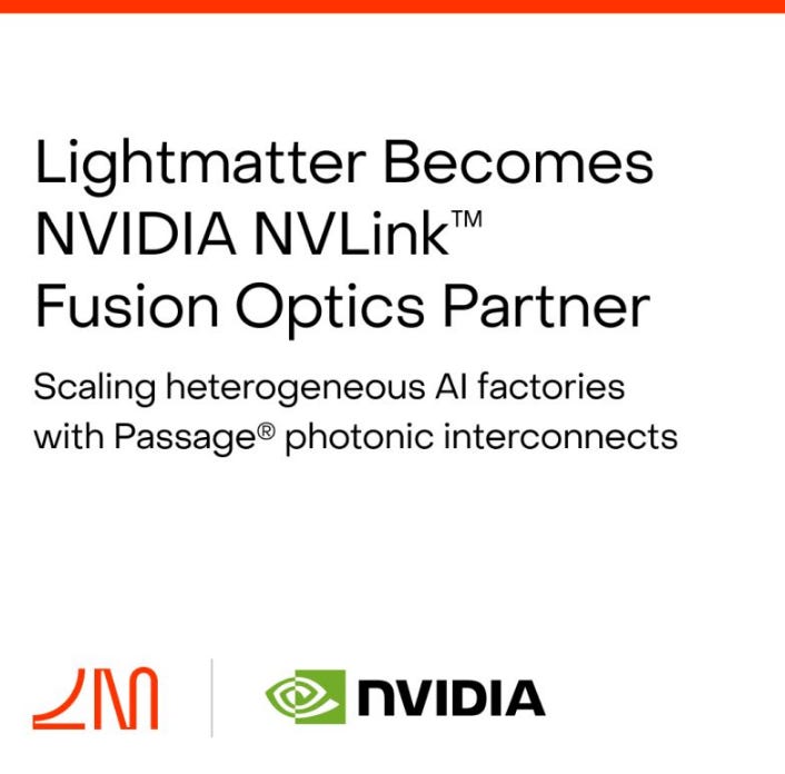
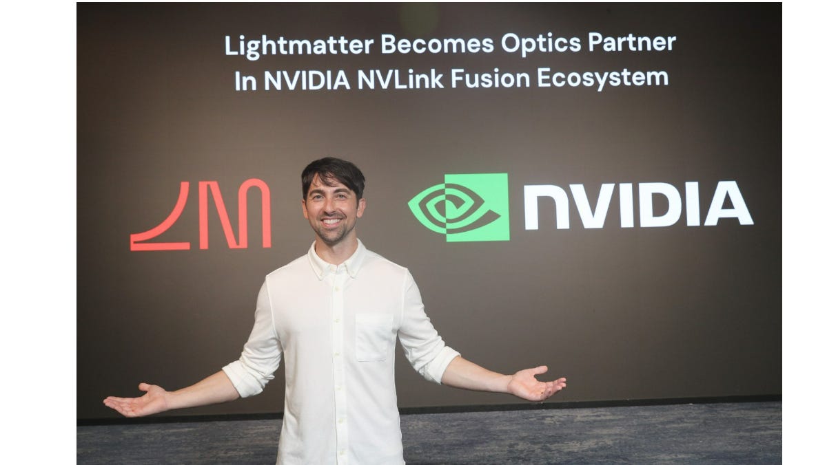
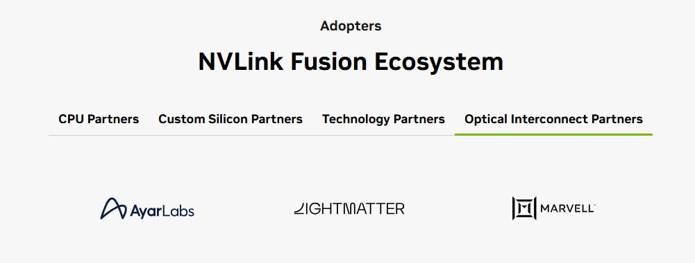
Lightmatter LinkedIn: The scale-up wall is real. To solve it, we’re integrating our industry-leading photonic interconnects into the ecosystem where it matters most. We are thrilled to announce that Lightmatter has become an optics partner in the NVIDIA NVLink™ Fusion ecosystem.
Scaling AI means scaling interconnects. As frontier models grow relentlessly, electrical interconnects are hitting fundamental physical limits on power, reach, and density, leaving massive amounts of compute capacity underutilized. Photonics is the only path forward.
Through this integration with NVIDIA's advanced system architecture, custom and semi-custom accelerators will connect to NVIDIA switch silicon via our Passage® co-packaged optics (CPO) and near-packaged optics (NPO)—powered by our Guide® VLSP™ lasers and industry-first bi-directional technology. This enables hyperscale customers to build AI factories with purpose-built silicon, unified by the highest bandwidth, lowest power optical fabric available from Lightmatter.
This is what we’ve been building toward since day one: empowering multi-rack scale-up clusters with the industry’s most advanced photonic interconnects, accelerating frontier AI model training and inference to unprecedented speeds.