

Lightmatter Passage : A 3D Photonic Interposer for AI
Original Article by SemiVision Research (TSMC , Nvidia , Lightmatter )

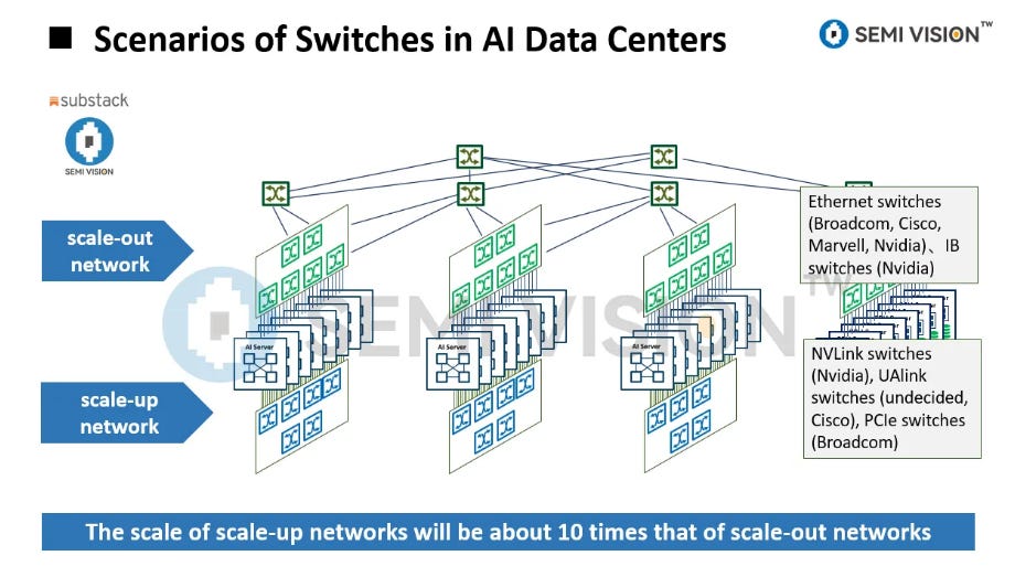
Scale-Up Challenges in Modern AI Training
Technical Background and Challenges
Over the past decade, the scale of AI models and their computational demands have grown exponentially—from early models with only a few million parameters to today’s models with hundreds of billions or even trillions. For instance, training large language models such as GPT-3 and GPT-4 typically requires thousands of GPUs in scale-out distributed systems to complete within a reasonable time. However, this expansion approach faces significant challenges.

On one hand, the slowdown of Moore’s Law has limited improvements in single-chip performance. On the other hand, multi-node distributed training introduces massive data communication overhead and synchronization delays, making network bandwidth a critical bottleneck. NVIDIA CEO Jensen Huang has noted that the computational demand for the latest AI training and inference workloads has surged by as much as 100x compared to expectations just a year earlier.
As a result, modern large-scale AI training is caught in a dilemma between Scale-Up (maximizing single-node performance) and Scale-Out (expanding horizontally across many nodes). Relying solely on massive GPU clusters leads to severe networking bottlenecks and soaring power consumption, while depending on single-node performance gains runs into limits of semiconductor scaling, thermal management, and power density.
Overall, in the post-Moore’s Law era, overcoming the dual bottlenecks of compute and communication has become a shared challenge for the entire industry.
Passage Technology Details
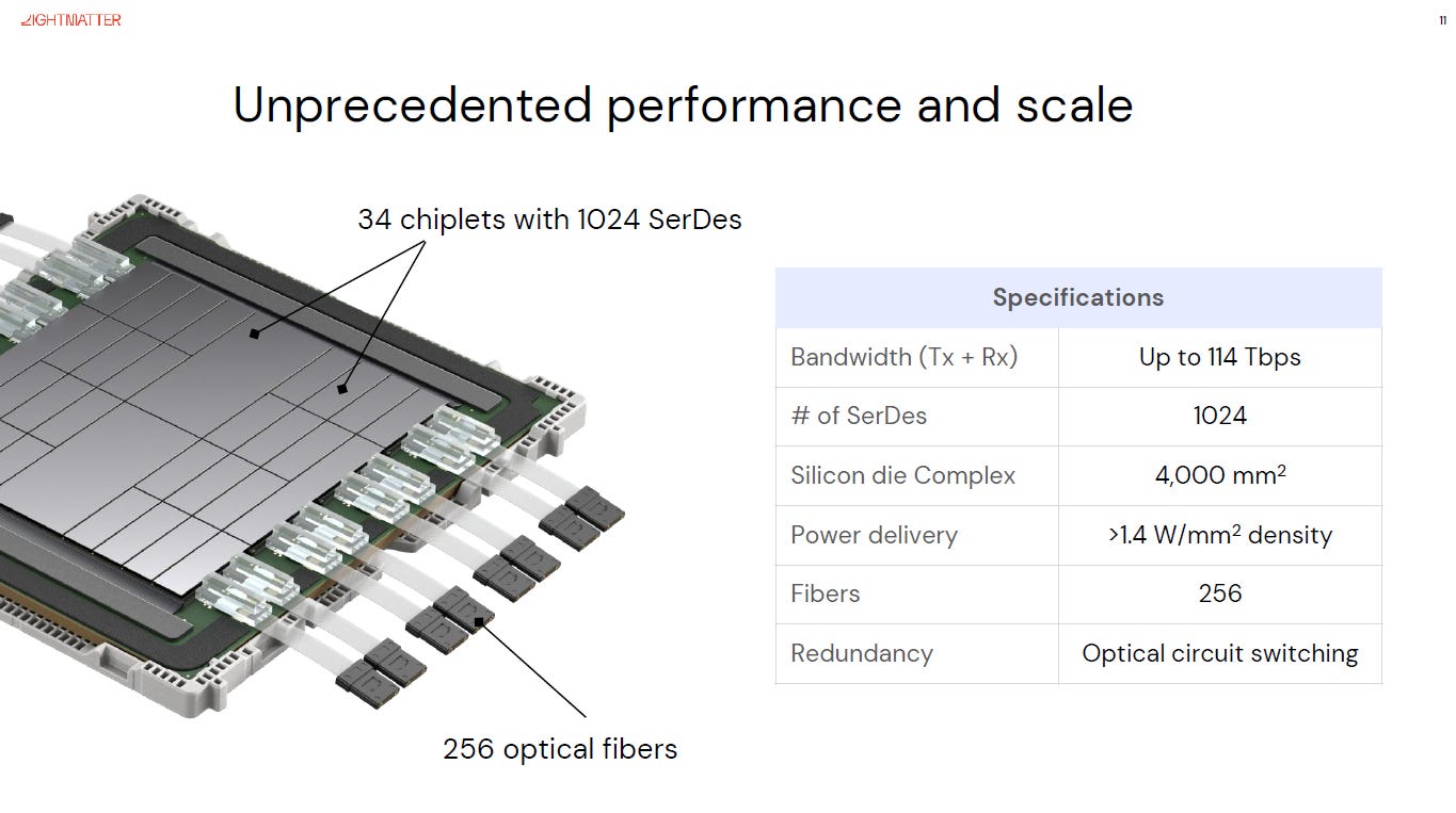
Lightmatter has identified that today’s primary bottleneck lies in insufficient interconnect capabilities across chips. To address this, the company introduced the Passage M1000 “superchip” platform, built on photonic technology to overcome critical Scale-Up barriers. The Passage M1000 employs an innovative 3D photonic stacking architecture, integrating up to 34 chiplets on a single photonic interposer, with a total equivalent die area reaching 4,000 mm²—surpassing the traditional reticle limit of a single chip.
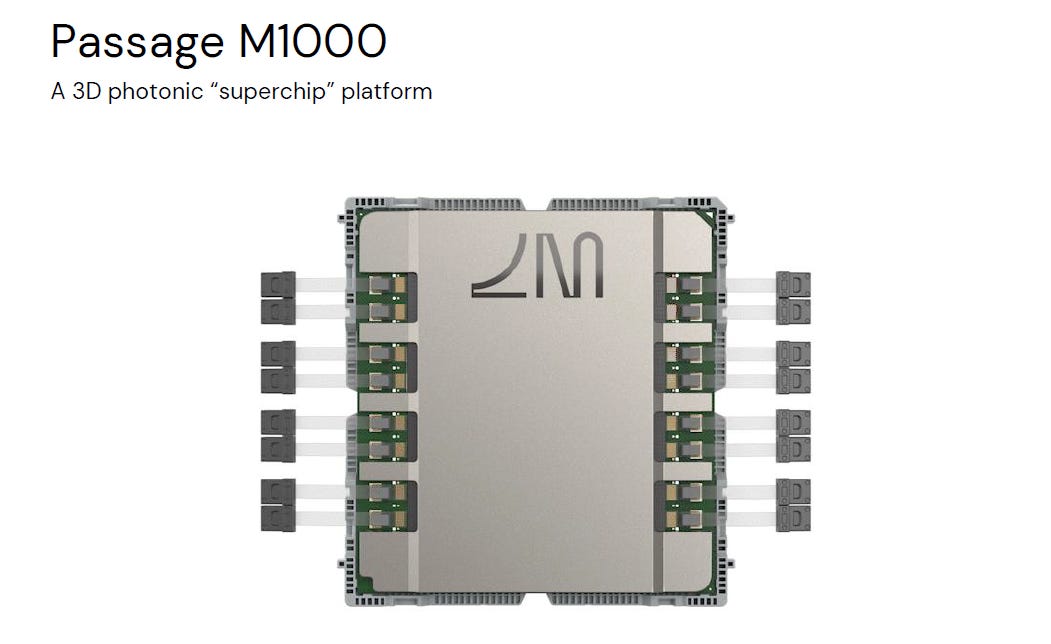
This approach enables the Passage platform to deliver unprecedented interconnect bandwidth: 114 Tbps of total bidirectional bandwidth (Tx+Rx) and 1,024 high-speed SerDes lanes. This means each integrated compute chiplet can access multi-terabit-per-second I/O bandwidth, effectively breaking through the conventional bottleneck of periphery-limited I/O pins on monolithic chips. As Lightmatter’s presentation put it: “We need more than 100× the bandwidth; a new paradigm is imperative.”
By leveraging its photonic stack, Passage allows numerous chiplets to share a high-speed optical communication backplane, collaborating with near-monolithic efficiency. This represents a new path forward in tackling modern AI Scale-Up challenges.
Photonics AI Processor in Nature: A Comparative View
A paper published in Nature validated the feasibility of photonics for AI acceleration from another perspective. The study showcased the first photonic processor capable of executing advanced neural networks such as ResNet and BERT, achieving accuracy close to that of 32-bit floating-point digital accelerators across multiple complex tasks.
This photonic processor employed a multi-chip integrated package, vertically combining six chips within a single package (four 128×128 photonic tensor cores, PTCs, plus two 12nm digital control interfaces, DCIs). High-speed interfaces connected the photonic compute chips with the electronic control chips, boosting system integration and computational efficiency.
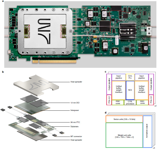
The design demonstrated that high-density packaging and vertical opto-electronic interconnects can significantly improve energy efficiency without sacrificing accuracy. In testing, the processor achieved 65.5 trillion 16-bit operations per second, consuming only ~78 W of electrical power plus 1.6 W of optical power. The Nature paper described its performance across workloads as achieving “near-electronic accuracy,” marking an important step toward the practical adoption of photonic computing in the post-Moore’s Law era.
Compared with Lightmatter’s Passage—which focuses on cross-chip interconnect—the Nature photonic processor emphasizes tensor computation at the photonic core level. Yet both approaches highlight photonics’ potential under Scale-Up challenges: the former offers a revolutionary data transfer architecture, while the latter proves that photonic compute cores can compete with electronic accelerators. Together, they suggest a future where photonic interconnect networks link multiple photonic/electronic compute cores, forming a new class of AI supercomputing platforms.
Comparison with Other Industry Players
As AI training continues to scale, other major players in the industry have taken different approaches to address the Scale-Up challenge:
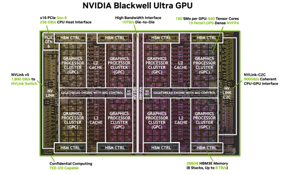
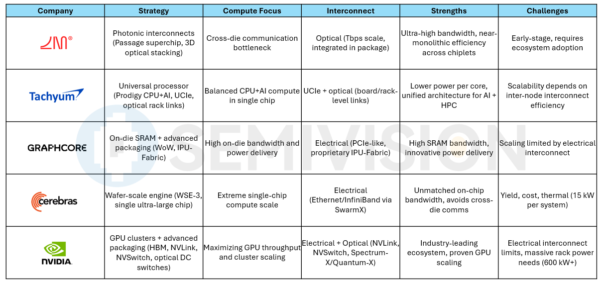
NVIDIA: NVIDIA has continued along a path of GPU cluster expansion coupled with advanced packaging. Its latest-generation Blackwell Ultra GPU adopts a dual-die design with 208 billion transistors, delivering roughly 50% higher performance than its predecessor, the H100.
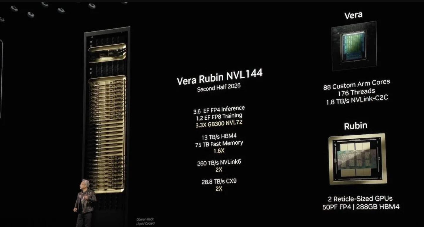
NVIDIA also plans to introduce the Vera Rubin superchip in 2025–2026, which will combine the next-generation “Rubin” GPU and “Vera” CPU. Built on a 3nm process and paired with HBM4 memory (offering 13 Tbps bandwidth, a major leap from the H100’s HBM3E at 8 Tbps), the Rubin GPU will deliver 50 PFLOPS (4-bit) inference peak performance, about 2.5× the Blackwell architecture. The follow-up Rubin Ultra, essentially packaging two Rubin GPUs together, is projected to reach 100 PFLOPS FP4 performance with nearly 1 TB of unified memory.
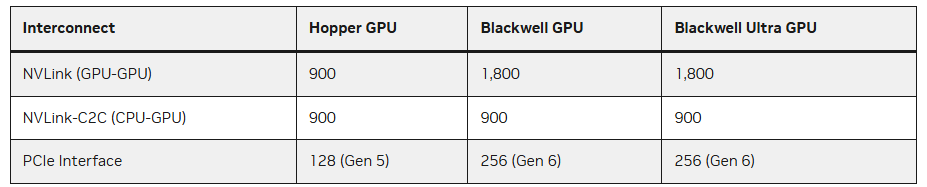
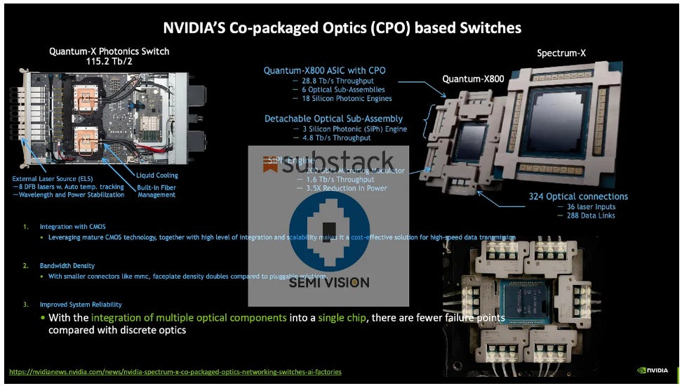
To support such massive compute power, NVIDIA is upgrading its interconnect technologies: the next-generation NVLink 6 point-to-point interface provides up to 3.6 Tbps total bandwidth per node. At the same time, NVIDIA is rolling out photonics-based datacenter switches (e.g., Spectrum-X, Quantum-X) offering port speeds up to 800 Gbps, capable of linking millions of GPUs.

Overall, NVIDIA continues to rely on powerful chip stacking (e.g., multi-chip modules combining Grace CPUs with Hopper GPUs), high-bandwidth HBM memory, and improved electrical interconnects (NVLink/NVSwitch) to achieve leading performance. However, the power and distance limitations of electrical interconnects are becoming increasingly prominent, requiring massive rack-scale and network infrastructure (with a single Vera Rubin rack consuming as much as 600 kW) to scale compute.
By contrast, Lightmatter’s Passage pursues optical interconnect to achieve tens to hundreds of Tbps networking capability within a single machine, effectively collapsing datacenter-level communication into a “superchip.” This architectural path holds the potential to simplify AI factory-style deployments and significantly improve efficiency.
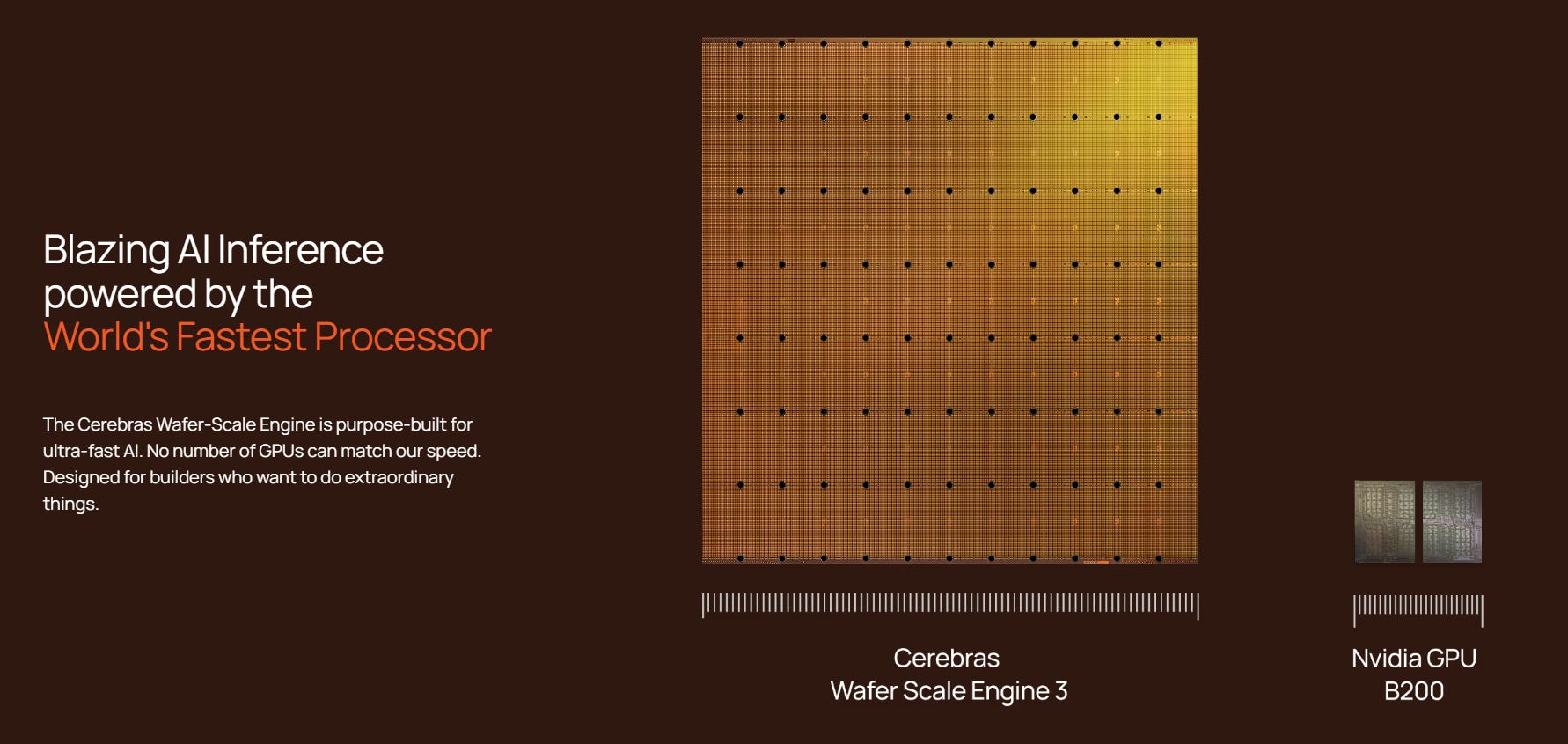
Cerebras: Cerebras has taken an extreme Scale-Up strategy by building the Wafer-Scale Engine (WSE), a single chip covering the entire wafer with a die area of 46,250 mm². The latest third-generation WSE-3 packs 4 trillion transistors, 900,000 sparse linear algebra cores, and integrates 42 GB of on-chip SRAM with an astonishing 21 PB/s of on-chip memory bandwidth.
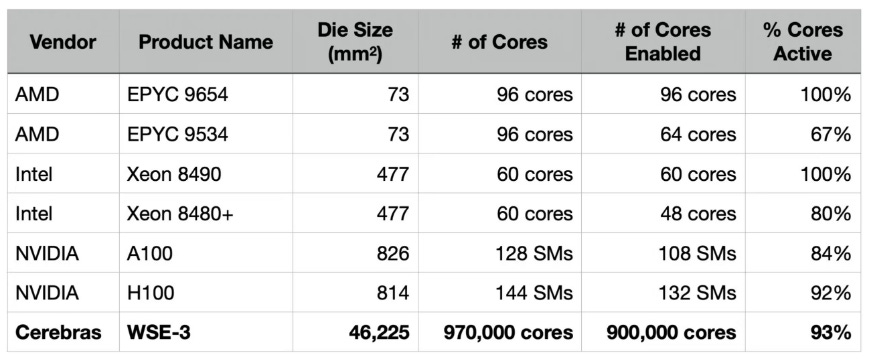
Such massive on-chip compute resources allow the WSE to train ultra-large models without requiring cross-chip communication. For example, the WSE-3 can fit the full weights of a 24-trillion-parameter model entirely within a single chip, with all data access occurring in a unified logical memory space. This delivers extremely high internal bandwidth density (21 PBytes/s—about 7,000× that of a conventional NVIDIA H100 GPU) and ultra-low latency, fundamentally different from multi-GPU clusters constrained by inter-node communication.
However, wafer-scale engines face challenges in manufacturing yield, thermal management, and cost. A single Cerebras CS-3 system consumes up to 15 kW, and its economies of scale lag behind standard GPUs. Cerebras is currently promoting its cluster solution, linking thousands of WSEs via SwarmX interconnect to build supercomputers. Yet, since scaling beyond a single wafer still relies on external high-end Ethernet/InfiniBand links rather than optical interconnects, and given the high overall cost, the approach faces hurdles.
By contrast, Lightmatter’s Passage, while not offering the same per-chip compute power as WSE, leverages optical interconnects to enable near-monolithic bandwidth communication across standard chiplets. This provides an alternative compromise: achieving giant-chip-like performance by tightly connecting smaller dies with dense optical links, potentially offering better cost efficiency and flexibility.
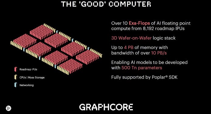
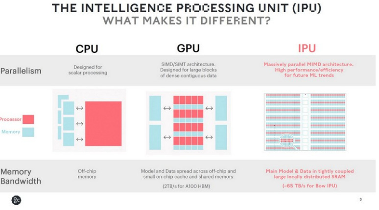
Graphcore: UK-based Graphcore focuses on innovations in advanced packaging and memory architectures. Its second-generation IPU (Colossus MK2) integrates 900 MB of distributed SRAM, delivering up to 260 TB/s of on-chip memory bandwidth through near-memory design.
In 2022, Graphcore introduced the Bow IPU, which adopted TSMC’s Wafer-on-Wafer (WoW) 3D stacking technology. It directly bonded a compute wafer containing 1,472 AI cores with a passive power-delivery wafer. This innovative packaging enabled the Bow IPU to operate at 1.85 GHz (vs. 1.35 GHz in the prior generation) at lower voltage, resulting in a ~40% performance boost and 16% improvement in energy efficiency. The principle lies in integrating deep trench capacitors and vertical TSVs within the power-delivery wafer, which supply stable power close to the compute cores, allowing higher clock speeds without increasing power consumption.
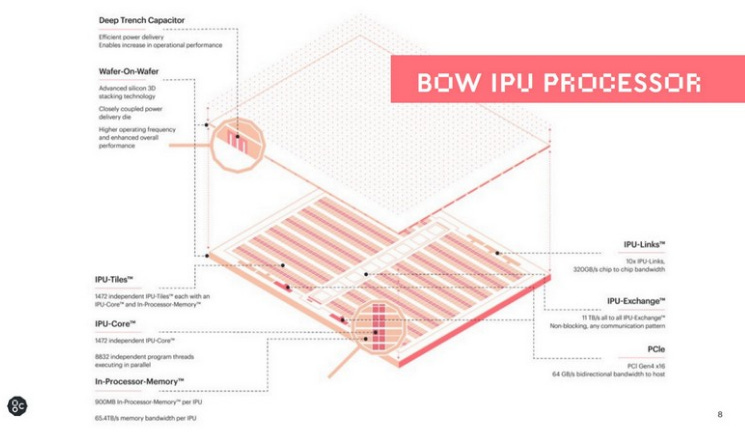
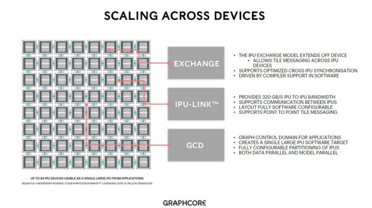
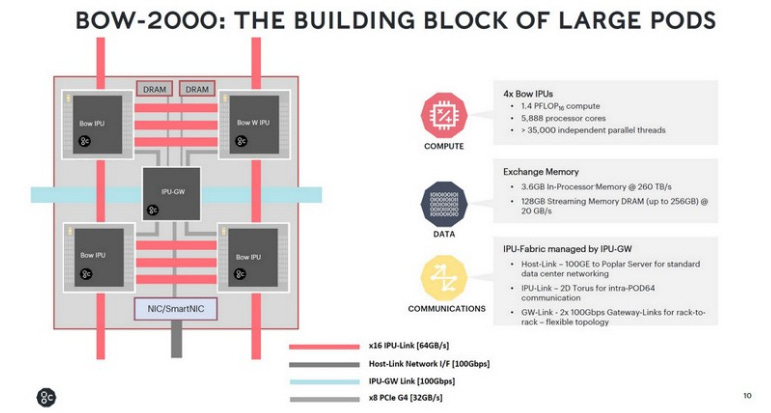
Graphcore’s architectural strength is that each IPU integrates large on-chip memory and thousands of small parallel cores, making it well-suited for models requiring extremely high memory bandwidth. Additionally, Graphcore provides its proprietary IPU-Fabric interconnect, enabling multiple IPUs to form Pod systems. However, communication between IPUs still relies on electrical interfaces (similar to PCIe or proprietary links), which becomes less efficient at very large scales (hundreds of chips or more) compared to optical interconnect solutions.
By contrast, Lightmatter’s Passage focuses on breaking the cross-die communication bottleneck, whereas Graphcore emphasizes on-die bandwidth and power delivery improvements through packaging innovation. In the future, combining Graphcore’s high-bandwidth on-chip SRAM design with Lightmatter’s chip-to-chip optical interconnect could potentially unlock even greater performance for distributed AI computing.
Tachyum: Tachyum is pursuing the “universal processor” route, aiming to create a new CPU architecture capable of handling both traditional HPC and AI workloads. Its upcoming Prodigy chip adopts an advanced multi-core design, reportedly offering up to 192 64-bit cores, with AI computing performance comparable to GPUs, while delivering better compute density and power efficiency.
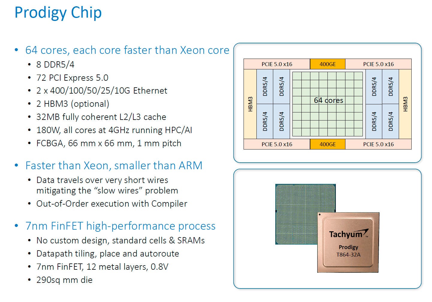
Tachyum emphasizes that its cores consume an order of magnitude less power than conventional processors, while supporting a unified architecture that can handle inference, training, and general-purpose computing tasks simultaneously. On the interconnect side, Tachyum has embraced the UCIe open chiplet interconnect standard, enabling future chiplet-based functional module expansion.
In addition, Tachyum is collaborating with optical connector vendors to introduce advanced fiber-optic high-speed connectivity into its Prodigy systems (e.g., co-developing OSFP-compatible optical modules with Senko) to enhance node-to-node communication bandwidth.
Compared with NVIDIA’s specialized accelerators, Tachyum’s strategy is to deliver balanced CPU + AI performance within a single chip, reducing data movement between heterogeneous devices. However, for ultra-large model training, Tachyum will still require clusters of multiple Prodigy chips, making inter-node interconnects a key determinant of scalability.
Tachyum’s focus on optical interconnects underscores its recognition of the limitations of traditional electrical links—an idea aligned with Lightmatter Passage’s philosophy of breaking communication bottlenecks through photonics. That said, Tachyum’s optical connectivity approach remains oriented toward board- or rack-level interconnect improvements, whereas Passage integrates optics directly into the package-level interconnect fabric, potentially achieving far greater integration depth and bandwidth density.
Analysis and Conclusion
Looking across the various approaches, the paths to scaling compute can be broadly divided into two categories: “building more powerful units” and “connecting more units more tightly.” NVIDIA, Graphcore, and Tachyum lean toward the former, using advanced process nodes, multi-die packaging, and architectural optimizations to create increasingly powerful compute units; Cerebras takes this to the extreme by delivering maximum performance on a single ultra-large chip.
However, as per-unit performance rises, data movement has become the bottleneck, prompting companies to also pursue the latter path: adopting faster electrical interfaces and even experimenting with optical interconnects. Lightmatter’s Passage exemplifies this trend, centering on 3D photonic interconnects to tackle the long-overlooked cross-die communication challenge, standing out among the many approaches to scaling compute. Compared with traditional electrical interfaces, Passage can deliver hundreds of Tbps of interconnect bandwidth at reasonable power, allowing horizontally scaled systems to operate almost as efficiently as scaling up a single giant chip.
Meanwhile, the Nature photonic AI processor provides validation from another angle, demonstrating that photonics can be used not only for communication but also for executing core arithmetic operations—with accuracy and energy efficiency competitive with electronic solutions. These advances complement each other and suggest a paradigm shift in AI acceleration: moving beyond sole reliance on transistor scaling, toward hybrid electronic-photonic architectures that break through performance ceilings.
In conclusion, under the Scale-Up challenges of modern AI training, a diversity of innovative approaches is flourishing. The emergence of Lightmatter Passage offers the industry a breakthrough pathway, delivering leapfrog improvements from the interconnect layer.
For Paid Member, SemiVision will discuss topics on:
Understanding Scale-Out vs. Scale-Up Computing
Distance Limitations of Copper Interconnects and Power Density Challenges
Passage 3D Photonic Stacking Solution Explained
UCIe and Interface Protocols
Packaging Technologies
Breakthroughs in Bandwidth Density and Energy Efficiency
Lightmatter Passage M1000: A Photonic Interconnect “Superchip”
