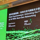
Nvidia : Integrating Photonic in HPC and Network Systems
Original Articles By SemiVision Research (IEEE ECTC , Nvidia , TSMC)
Redefining the Foundations of AI Datacenters — The Tipping Point of Photonic Integration Has Arrived
The exponential growth of generative AI has accelerated the transformation of datacenter architecture at an unprecedented pace. From xAI’s Colossus cluster—now deploying 100,000 H100 GPUs—to hyperscalers like Meta and Google building trillion-parameter GPU systems, the fundamental bottlenecks of AI infrastructure have shifted. It is no longer just about compute performance; communication and energy efficiency have become the new frontiers.
As traditional copper interconnects begin to hit the physical limits of bandwidth-distance product (BW × distance), optical communication has emerged as the critical enabler for the AI factory of the future. To support terabit-level bandwidth and massive inter-node connectivity, innovation must now move beyond the processor core and into the packaging and interconnect layers.
Against this backdrop, the Electronic Components and Technology Conference (ECTC) stands out as one of the world’s most influential forums for semiconductor packaging, advanced interconnects, and optical-electronic integration. Far more than a technical showcase, ECTC is a strategic platform where the global supply chain converges to align on next-generation architectures, materials, and scalability roadmaps.
Why ECTC Matters
Hosted by the IEEE Electronics Packaging Society, ECTC focuses on critical domains such as chiplet integration, advanced packaging, 2.5D/3D interconnects, thermal management, reliability assurance, and photonic co-packaging. It is widely regarded as the premier global venue for technical leaders from companies like TSMC, Intel, NVIDIA, Amkor, ASE, and Broadcom, alongside academic pioneers and system architects.
At the 2025 edition, NVIDIA’s unveiling of its Spectrum-X photonic switching platform and comprehensive CPO (Co-Packaged Optics) and CIO (Co-Integrated Optics) strategy marked a defining moment. From silicon photonic engines (SiPh), TSMC’s COUPE packaging, and 3D-stacked EIC/PIC integration to metrics such as power density, bandwidth per mm, laser count, and signal integrity—NVIDIA presented a holistic roadmap that redefines interconnect architectures for AI.
These advances herald the arrival of an “all-optical era” for hyperscale datacenter networks, where optics is no longer just a backend enhancement, but a core design element that determines performance, scalability, and reliability.
In the Era of Generative AI, How Will Photonic Integration Reshape Compute and Communication?
With model sizes and computational demands growing exponentially, from AlexNet in 2011 to PaLM in 2023, training workloads have surged from hundreds of TFLOPs to exa-scale demands. At ECTC 2025, NVIDIA Senior Research Scientist Nandish Mehta emphasized that photonic integration is now the linchpin to overcoming the bandwidth and energy bottlenecks of large-scale AI training systems. Through radical hardware innovation, photonics is not just an upgrade—it is the foundation for the next generation of AI infrastructure.
For our paid members, SemiVision will provide in-depth coverage and analysis of NVIDIA’s keynote at ECTC, highlighting key insights and industry implications
The Compute Explosion and Hardware Evolution Driven by Generative AI
The Dual Challenges of Modern AI Datacenters: Communication Bottlenecks and Power Constraints
Breakthroughs in Photonic Integration: From CPO to CIO
From CPO to CIO
Next-Generation Optical I/O: Innovations in Modulation and Energy Efficiency
CIO vs. Traditional CPO — Key Advantages:
From Copper to Embedded Optics: A Paradigm Shift in System Architecture


