Perspective on SerDes and CPO: PCB Material and Signal Routing Challenges Ahead
Original Article by SemiVision Research (TPCA Taiwan , TCPA Japan , EMC , Nvidia , Broadcom , Marvell , TSMC)
How Will Material Innovation Become the Core Breakthrough for AI Infrastructure as SerDes Advances to 224G?
The AI server and high-performance computing (HPC) sectors are entering an era of unprecedented I/O density and bandwidth requirements. At the heart of this evolution lies the SerDes (Serializer/Deserializer) interface. From the early 28Gbps NRZ and 56Gbps PAM4 to today’s 112Gbps and soon-to-be-commercialized 224Gbps SerDes, each leap in bandwidth has relied not only on IC design improvements but also on a deeper, more complex challenge: materials innovation. At ultra-high frequencies, maintaining signal integrity, controlling insertion loss, and ensuring reliability amid thermal and mechanical stress all depend heavily on advanced substrate materials.
As generative AI and large language models evolve at an unprecedented pace, data center interconnect architectures are facing critical new challenges. With model sizes expanding into the hundreds of billions—and even trillions—of parameters, bandwidth bottlenecks and energy efficiency have become key constraints on scalable AI compute infrastructure. Marvell, a global leader in data infrastructure semiconductors, is redefining the interconnect paradigm for the AI era through its deep expertise in high-speed SerDes IP and silicon photonics technologies.
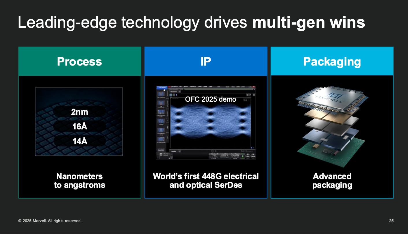
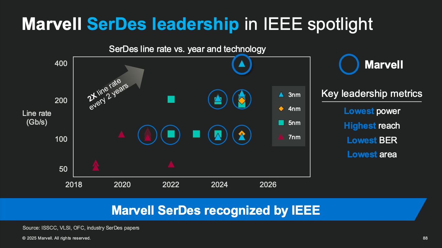
Since 2018, Marvell has led the industry in SerDes development, culminating in the demonstration of its 3nm, 224Gbps SerDes at OFC 2025. With innovations including optical retimers and gearboxes, Marvell is pushing toward 400+ Gbps per lane performance. These advancements demonstrate industry-leading metrics in ultra-low power (<0.1 pJ/bit), ultra-high bandwidth density (50+ Tbps/mm), and lowest bit error rates (BER)—solidifying its critical role in Co-Packaged Optics (CPO) and Die-to-Die (D2D) interconnect applications.
But Marvell’s strategy goes far beyond link-level IP. Its comprehensive IP portfolio spans SerDes, silicon photonics, dense SRAM, custom HBM, and advanced packaging—aligned with TSMC’s CoWoS platform and JEDEC standards. This enables scalable XPU and XPU attach solutions that support custom AI accelerators and heterogeneous deployment models across cloud and enterprise.
On the optical interconnect front, Marvell’s silicon photonics platform has seen multiple generations of field deployment—from 100G and 400G modules to the upcoming 1.6T solutions targeted for commercialization in 2026. By integrating photonics and electronics on a single silicon system and deploying 3D light engines on the package’s reverse side, Marvell’s CPO solutions offer up to 6.4Tbps per engine and 25.6Tbps in multi-engine configurations—providing essential scalability for data centers.
As SerDes and optical links move from board edges into chip cores, Marvell stands among the few full-stack providers capable of integrating electrical, optical, packaging, and software domains. Marvell’s IP leadership and co-design capabilities position it at the forefront of next-generation custom infrastructure and high-speed interconnect ecosystems.
In this wave of technological disruption, Taiwan-based Elite Material Co., Ltd. (EMC) has emerged as a key global driver of high-speed material innovation. Starting with halogen-free green HDI materials, EMC has now expanded its portfolio to cover next-generation packaging technologies such as AI servers, Co-Packaged Optics (CPO), Near-Package Optics (NPO), FCBGA, and Antenna-in-Package (AiP). EMC’s strategy demonstrates its remarkable transition from low-frequency mobile devices to ultra-high-speed, mission-critical infrastructure — from smartphones to space.
As AI servers compress transmission distances and signal edges become more fragile, the dissipation factor (Df) and coefficient of thermal expansion (CTE) are becoming critical indicators of material suitability. At 112Gbps PAM4 (~28GHz), traditional FR-4 or standard HDI materials are already stretched to their limits. With 224Gbps PAM4 pushing operating frequencies to ~56GHz, SerDes design now intersects with materials science, packaging architecture, and signal integrity engineering.
EMC has achieved a major breakthrough at this critical juncture. Its low-Df material EM-S532K features a Df of just 0.0037 — a substantial improvement over the previous-generation EM-S526 (Df 0.0081), reducing insertion loss by over 35% at 80GHz. To meet the demands of CPO architectures, where silicon photonics and electrical components are tightly co-packaged, EMC has also introduced materials such as EM-S570K3 and EM-S572T, featuring ultra-low CTE (<2 ppm/°C) and high modulus (>35 GPa) — essential properties for precise mechanical matching and long-term reliability in SerDes + SiPh integration.
This wave of materials innovation is also reflected in EMC’s business trajectory. From the first materials boom triggered by smartphones in 2003, to the current transformation driven by AI servers since 2021, EMC’s annual revenue growth has jumped from $74 million per year to over $230 million annually. The company’s total revenue is projected to reach $2.5 billion in 2025, underscoring the explosive demand for next-generation high-speed substrates.
Global Demand for High-End CCL Surges Rapidly
With the rise of high-speed computing and communication applications, the global copper-clad laminate (CCL) market is undergoing a structural shift. While growth in the traditional mid-to-low-end FR-4 segment is slowing, demand for high-frequency, high-speed advanced CCLs is increasing significantly.
In particular, the advent of AI servers in cloud data centers and the transition to 800G network switches has driven many manufacturers to adopt ultra-low-loss materials like M8-grade CCLs (e.g., Panasonic Megtron 8). Launched in 2022, Panasonic’s Megtron 8 supports 800GbE high-speed networks and features a dielectric loss factor (Df) of approximately 0.0015—about 25% lower transmission loss compared to the previous-generation Megtron 7 (Df ≈ 0.002).
These M8+ high-performance materials, known for their low dielectric constant and minimal signal loss, are becoming essential for next-generation high-speed PCB designs. According to a CCL industry report released by Goldman Sachs on November 20, 2024, the global high-end CCL market is projected to achieve a compound annual growth rate (CAGR) of 26% from 2024 to 2026—significantly outpacing the overall CCL market’s growth rate of around 9%.
Regional Market Development:
The supply of high-end CCLs is primarily concentrated in Asia, particularly in Taiwan, South Korea, and Japan. While Chinese manufacturers hold a strong position in the mid-to-low-end CCL market, they still lag behind in both technology and certification when it comes to ultra-high-frequency M8-grade materials. As a result, this segment is currently dominated by suppliers from Taiwan, Korea, and Japan.
Due to ongoing U.S.-China tech tensions, American tech giants increasingly rely on supply chains based in Taiwan, Korea, and Japan for their AI servers and high-speed network switches. This shift has driven up shipments of high-end CCLs from Taiwanese manufacturers. Key players in the M8-generation supply chain include Taiwan's EMC, TUC and Iteq, South Korea’s Doosan, and Japan’s Panasonic, forming the core competitive group in the current high-end CCL market.
When SerDes Advances to 224G, How Does Materials Innovation Become the Core Breakthrough of AI Infrastructure?
Today’s AI servers and high-performance computing (HPC) systems are facing unprecedented demands for I/O density and bandwidth. One of the key enabling technologies behind this shift is the SerDes (Serializer/Deserializer) interface. From early 28Gbps NRZ and 56Gbps PAM4 to 112Gbps and now the emerging 224Gbps SerDes, each leap in bandwidth isn’t just about IC design—it critically depends on materials innovation. Maintaining signal integrity, managing insertion loss, and enduring mechanical stress under high-frequency conditions all require advanced substrate materials.
Amid this wave of technological change, Taiwan-based Elite Material Co., Ltd. (EMC) has emerged as a global leader in high-speed base materials. Originally known for its halogen-free HDI materials, EMC has now extended its product coverage to support emerging advanced packaging architectures including AI servers, Co-Packaged Optics (CPO), Near-Package Optics (NPO), FCBGA, and Antenna-in-Package (AiP). This showcases EMC’s broad technical range—from mobile to aerospace applications—and its strategic transformation.
For AI servers employing SerDes, shorter transmission distances and fragile signal edges make Df (Dissipation Factor) and CTE (Coefficient of Thermal Expansion) the key material metrics. At 112Gbps PAM4 (~28GHz), traditional FR-4 and HDI materials already struggle. With 224Gbps PAM4 pushing frequencies to 56GHz, SerDes becomes a multidisciplinary challenge involving materials science, packaging, and signal engineering.
EMC has achieved breakthroughs with materials like EM-S532K, reducing Df to 0.0037 (compared to EM-S526’s 0.0081), cutting insertion loss by over 35% at 80GHz. For CPO systems requiring photonic-electronic co-packaging, new materials like EM-S570K3 and EM-S572T feature ultra-low CTE (<2 ppm/°C) and high modulus (>35 GPa), supporting precise alignment and reliability.
This materials revolution is reflected in EMC’s revenue trajectory—from a $74M annual growth rate during the smartphone boom of the 2000s to over $230M per year since the AI server boom in 2021, with total revenue projected to reach $2.5B by 2025.
According to Prismark's 2023 report, EMC has become the world’s No.1 in the high-speed substrate market with a 28% share, surpassing Japan’s Panasonic and Taiwan’s TUC. EMC is also expanding in high-reliability sectors such as AI servers, network switches, LEO satellites, ADAS, and defense electronics.
More importantly, EMC is not only improving core material performance but also enhancing integration capabilities with advanced packaging. For example, the EM-S532K series for AiP improves high-frequency insertion loss and mitigates thermal stress caused by structural asymmetries in packaging due to its low CTE. This allows HDI-based materials to compete with fan-out and even glass interposer platforms in 5G/Wi-Fi 7 modules—offering a high-performance, scalable, and cost-effective solution.
In this context, materials are no longer passive enablers but strategic drivers of AI and high-speed architecture innovation. From SerDes specs to packaging and yield management, EMC embodies a "materials-driven architecture transformation" approach—cementing Taiwan’s role in the global high-frequency materials landscape.
Looking ahead, as CPO enters production and 1.6TbE and ultra-high-speed switches become mainstream, SerDes and silicon photonics will push materials science to new frontiers. Leaders like EMC, with systemic design thinking across Df, CTE, modulus, and packaging compatibility, will become the invisible core enabling next-gen data centers, EVs, satellite communications, and AI chips. This is not just a market opportunity—it is a redefinition of industry positioning.
This article will integrate PCB-level perspectives on SerDes design and explore key challenges in signal integrity (SI) and power integrity (PI). It will also provide a holistic view of electromagnetic compatibility -driven layout strategies. Our goal is to explain why AI chip system design is no longer just a chip-level issue — it also requires deep consideration of PCB architecture, materials, and system-level interactions.
Furthermore, the article will deliver a comprehensive analysis that bridges chip, board, and material layers, with updated insights into high-speed transmission strategies currently being adopted by companies like Broadcom and Marvell.
For Paid Members ,SemiVision will discuss topics on
What is CCL?
SerDes Bandwidth Evolution and Its Systemic Implications in the AI and Silicon Photonics Era
Comprehensive Understanding of Impedance Matching and Loss Budgeting: The Core Battlefield of Signal Integrity in the High-Speed Design Era
Power Integrity (PI) First: The Foundation of System Reliability
SI Comes Next: Precision in Impedance and Loss Budget
The Design Loop: From PI to SI to Material Strategy
EMC Group Sales Growth – From Foundation to Acceleration
EMC Global Ranking in 2023 – Market Leadership in HDI and Halogen-Free Laminates
EMC – Global No.1 in High-Speed Laminate (2023)
EMC Product Roadmap for FCBGA/SiP
What is AiP?
Key Industry Trends Reflected in the Image in AiP
Key Advantages of EMC’s HDI-Based Solutions
Chart Analysis: Insertion Loss vs. Frequency
Five Generations of Optical Module Evolution (2022–beyond)
Silicon Photonics (SiPh): The Key Enabler
Mega Trend in Optical Module material viewpoints from EMC
High-Speed SerDes and Optical Interconnect Trends


