


Silicon-organic Hybrid Electro-optic Modulators for Next Generation Optical Interconnects
Original Article By SemiVision Research (Foxconn, SilOriX ,Black Semiconductor , Lab 91 ,TSMC ,Nvidia , HyperLight )

The silicon photonics industry marks the dawn of a new technological era—one defined by extreme complexity and deep cross-disciplinary integration. It is often considered one of the most demanding sectors in semiconductor advancement due to the broad spectrum of expertise required.
To truly understand the silicon photonics ecosystem, one must first be familiar with advanced packaging, since all photonic devices must eventually be integrated into hybrid electronic-photonic modules. Equally essential is RF signal processing, which governs how high-speed modulators and drivers interact with the transmission system. Then comes optical physics, the foundation behind waveguide design, mode confinement, coupling efficiency, and other critical photonic behaviors. Finally, a strong grasp of materials science and fabrication reliability is indispensable, as the performance of optical modulators and receivers is fundamentally dictated by material properties—especially their electro-optic response, thermal stability, and process compatibility.

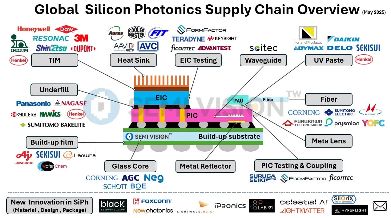
Together, these factors make silicon photonics a high-barrier, multidisciplinary frontier.
Currently, mainstream data centers still rely heavily on copper interconnects. But as the industry inevitably shifts toward optical interconnect architectures, we will witness a profound transformation. Particularly when modulators move beyond silicon-based designs, the importance of materials innovation will take center stage. New materials—such as lithium niobate, EO polymers, or hybrid organic-silicon platforms—will redefine the boundaries of performance, energy efficiency, and integration.
For readers unfamiliar with this transition, we encourage you to revisit our earlier deep-dive articles on silicon photonics, SOH, TFLN, and EO polymer modulators to gain a more comprehensive understanding of the road ahead.

A Comparative Outlook on Mainstream Electro-Optic Modulator Technologies
SemiVision has conducted a structured comparison of the leading electro-optic modulator (EOM) technologies currently shaping the photonics industry. The analysis covers five major platforms:
Silicon-Organic Hybrid (SOH) – exemplified by innovators like SilOriX
Thin-Film Lithium Niobate (TFLN)
Indium Phosphide Electro-Absorption Modulated Lasers (InP EML)
Silicon Mach-Zehnder Modulators (SiPh MZM)
Electrically Tunable Metasurfaces (ETMs) – emerging materials and structures
For short-reach IM-DD high-speed modules (400G–800G/lane), SOH and TFLN stand out as the most promising contenders:
SOH offers unmatched compatibility with CMOS backend processes and supports sub-1V driver-less operation. Lab demonstrations have shown SOH-based modulators achieving over 500 Gbps per channel, making it ideal for next-generation LPO modules and AI/HPC interconnects.
TFLN excels in bandwidth (exceeding 110 GHz) and material stability, making it highly suitable for driver-based architectures and coherent systems. It is rapidly advancing toward commercial maturity, especially in the 400G/lane class.
Meanwhile, other platforms are increasingly specialized in their roles:
InP EML remains a cornerstone of commercial 100G/200G optical modules, valued for its integration of laser and modulator functions. However, as data rates move toward 400G/lane, InP solutions face significant limitations in packaging density and thermal management.
SiPh MZM continues to dominate in low-cost, mass-produced LPO designs. That said, its limited bandwidth and relatively high Vπ necessitate hybrid approaches—such as SiPh+TFLN or SiPh+SOH—to stay competitive in higher-performance applications.
Electrically Tunable Metasurfaces (ETMs), while not yet viable for high-speed data center optics, show potential in emerging use cases such as reconfigurable beam steering, flexible photonics, and LiDAR. Their value lies in multifunctionality and form-factor innovation rather than raw modulation speed.
The transition to 400G–800G/lane optical modules is not just a matter of higher bandwidth or lower energy per bit. It marks a shift in system architecture—where integration strategy, process compatibility, and materials innovation will determine success. With SOH and TFLN already demonstrating leading-edge performance, silicon photonics and InP must increasingly rely on hybrid integration to keep pace with the next wave of optical interconnect demands.
If we categorize electro-optic modulator technologies based on their core material systems, they can be broadly divided into four types: Silicon-based modulators, Graphene modulators, Thin-Film Lithium Niobate (TFLN) modulators, and Organic Electro-Optic (OE) Polymer modulators.
Silicon-based modulators are suitable for cost-sensitive, standard optical modules, but their performance is inherently limited. To meet next-generation requirements, they increasingly rely on hybrid approaches such as SiPh+TFLN or SiPh+OE Polymer integration.
Graphene modulators demonstrate breakthrough potential due to their ultra-high-speed response and flexibility, making them ideal for flexible electronics and ultra-fast signal processing. However, material stability and manufacturing maturity remain key challenges before widespread adoption.
Amid the global wave of semiconductor and materials innovation, Black Semiconductor and Lab91 are both actively advancing their distinct strategies in the field of graphene and TMD based on device . Though originating from different backgrounds, both companies share a common vision: unlocking the potential of graphene in enabling next-generation high-bandwidth, low-power communication and computing architectures.
Black Semiconductor is focused on developing an integrated graphene platform that combines electronic and photonic data transmission. Through its Integrated Graphene Photonics (IGP) technology, the company aims to overcome the limitations of conventional metal interconnects by enabling faster and more energy-efficient chip-to-chip communication. Their recent acquisition of Dutch graphene material specialist Applied Nanolayers has accelerated their vertical integration capabilities—from material synthesis to process development. The company plans to launch its pilot production line, FabONE, in 2025 as a step toward commercialization.
Meanwhile, Lab 91 is working on developing Transition Metal Dichalcogenide (TMD) based devices in various application domains, including optoelectronic/photonics. An example implementation maybe a monolithically integrated on-chip laser (replacing InP and associated complex packaging steps) or electro-optic SERDES, taking advantage of MoS2’s tunable bandgap (in monolayer form, it has a direct bandgap of 1.6 to 1.8 eV, which compares favorably to InP which has s direct bandgap of 1.3 eV)
TFLN is currently one of the most mature and stable high-performance platforms, particularly well-suited for wide-bandwidth transmission and high-end optical packaging in both coherent and IM-DD applications.
Amid the rapid evolution of high-speed optical communication and advanced packaging technologies, HyperLight has emerged as a standout innovator in the silicon photonics landscape. Spun out from cutting-edge research at Harvard University, HyperLight has pushed thin-film lithium niobate (TFLN) technology to new performance frontiers—delivering modulators with ultra-low loss, high bandwidth, and low driving voltage, all while maintaining compatibility with CMOS fabrication processes. Through its proprietary ultra-thin LN bonding techniques and advanced photonic designs, HyperLight is not only breaking through the limitations of traditional silicon-based modulators but also paving the way for next-generation data centers, AI interconnects, and photonic computing architectures.


In the evolving field of photonic integration, heterogeneous platforms that combine Silicon (Si), Silicon Nitride (SiN), and Thin-Film Lithium Niobate (TFLN) are emerging as a promising foundation for high-performance optical systems. This tri-layer architecture leverages the unique physical properties of each material to enable high-speed, low-loss operation while maintaining compatibility with scalable semiconductor manufacturing processes.
At the foundation, Silicon (Si) is primarily used for photodetectors (PDs). Silicon exhibits excellent absorption in the near-infrared range, particularly around 1310 nm and 1550 nm, which are standard telecom wavelengths. When integrated with Germanium (Ge), silicon enables the fabrication of high-efficiency, low-dark-current photodetectors capable of supporting fast data reception. This makes it highly suitable for applications in data centers, optical links, and advanced sensing systems.
Silicon Nitride (SiN) serves as the passive photonic layer, providing low-loss waveguiding and efficient coupling structures. SiN offers a broad transparency window—from visible to mid-infrared wavelengths—and exhibits low optical loss, minimal nonlinear absorption, and excellent thermal stability. These attributes make it ideal for long-distance signal routing, fiber coupling, and power handling in high-density photonic circuits. SiN also facilitates mode conversion and efficient interface with external optical systems, reducing packaging complexity and overall insertion loss.
At the core of modulation, Thin-Film Lithium Niobate (TFLN) is employed due to its strong Pockels effect, which is essential for high-speed electro-optic modulation. Through techniques like micro-transfer printing or low-temperature bonding, TFLN films can be integrated onto SiN waveguides to form compact, high-bandwidth Mach-Zehnder Modulators (MZMs). Recent studies have demonstrated that such hybrid modulators can exceed 100 GHz of bandwidth while achieving a low Vπ·L product in the range of 3–4 V·cm, making them highly energy-efficient and suitable for future communication demands.
The realization of this tri-material stack requires advanced process control and precise alignment across multiple optical layers. Microfabrication techniques, including transfer printing and low-temp bonding, enable accurate placement and stable adhesion of diverse materials while preserving their intrinsic optical properties. Importantly, these techniques are compatible with standard wafer-scale CMOS processes, facilitating mass production and integration into next-generation optical systems.
In summary, the Si + SiN + TFLN heterogeneous integration platform offers unmatched flexibility and performance for advanced photonic integrated circuits (PICs). This architecture is particularly well-suited for data center interconnects, photonic AI accelerators, LiDAR systems, and monolithically integrated optoelectronics. As fabrication technologies continue to mature, this multi-material photonics platform is poised to play a central role in the evolution of next-generation computing and communications infrastructure.
OE Polymer modulators (e.g., SilOriX) stand out for their ultra-low energy consumption and CMOS-level drive compatibility, making them highly attractive for LPO architectures, driver-less operation, and next-generation AI/HPC optical interconnects.

Foxconn Research Institute holds a leading position in the field of photonics, particularly in silicon photonics (SiPh). Its research outcomes play a pivotal role in advancing Taiwan’s photonics and optoelectronics ecosystem. As one of the few industrial institutions with in-house silicon photonics integration capabilities, Foxconn’s research team is actively engaged not only in fundamental device design, but also in cutting-edge areas such as high-speed modulators, photonic-electronic integration, and optical packaging.
In addition, Foxconn Research is collaborating closely with the NYCU team on innovative research in heterogeneous photonic integration, material platform development, and optical module systems. Together, they form a highly synergistic research force driving progress in the field. In the near future, we will introduce a series of selected research papers and technical milestones to explore their potential impact and strategic value in the evolution of next-generation optical interconnect technologies.
SemiVision will provide insights into SilOriX’s current perspectives on the use of polymer-based technologies in the silicon photonics industry. This reflects a broader industry trend, as many discussions in global photonic tech forums are increasingly centered on “Beyond Silicon” modulators. Both international and Taiwanese supply chains are actively investing in the next generation of silicon photonics, recognizing that the future of this field will be materials-driven. This shift toward advanced material integration is expected to be a key catalyst in the continued growth of silicon photonics.
A Strategic Enabler for the AI and Big Data Era: SilOriX and the Rise of Next-Generation Electro-Optic Modulators
A New Landscape in Electro-Optic Modulation: SOH, TFLN, and Electrically Tunable Metasurfaces
Challenges and Opportunities in the AI Era: How Electro-Optic Modulators Can Break the Interconnect Bottleneck
Core Advantages of SilOriX’s SOH Modulator
Feature of Organic Electro-Optic Material
The Perfect Combination of High Performance and Low Power Consumption
SilOriX’s SOH Process Chain: A Full-Stack Platform from Molecular Design to System Integration
Flexible Commercial Models and Ecosystem Interfaces
SilOriX Core Technology Insight: Architecture of the Silicon-Organic Hybrid (SOH) Modulator
Proven Stability and Reliability in SOH Modulator
Bandwidth Optimization Breakthrough: How SilOriX Achieves >100 GHz High-Speed Modulation
SilOriX: A Strategic Enabler for Optical Interconnects in the AI Era
SilOriX SOH Modulator — A High-Efficiency, High-Speed, and Scalable Breakthrough for Optical Interconnects
