Material-Driven Revolution: Enabling High-Speed Modulation in Silicon Photonics
Original Article by SemiVision Research (UMC,TSMC,Nvidia,Lightwave Logic,HUST,ETH Zurich,McGill University & Lumiphase,KIT & SilOriX, Foxconn )

SemiVision has published a wide range of in-depth articles on silicon photonics, aiming to drive broader understanding and engagement across the ecosystem. As we look ahead, it’s time to seriously consider what the future roadmap might look like — including advancements such as 400G per lane interconnects, the high-frequency performance of Ge photodetectors (Ge PDs), and breakthroughs in next-generation materials.
This article will focus on emerging trends in high-frequency photonic components, with particular attention to innovations in materials science.
From novel electro-optic platforms and hybrid material integration to thermal stability improvements and low-loss modulation, we will explore the key technologies that could redefine silicon photonics in the next decade.
Over the past decade, with global internet traffic experiencing exponential growth, high-frequency optical modulation technology has emerged as a critical driver for upgrading communications and data center infrastructure. The rapid proliferation of high-resolution streaming, B5G technologies, cloud computing, and IoT devices has increasingly rendered traditional silicon photonics-based fiber networks insufficient to meet the future demands for Tbit/s-level data transmission.
To address this impending bandwidth revolution, the industry is striving to break through the limits of symbol rate, advancing from 50 Gbaud and 100 Gbaud toward 200 Gbaud and even beyond 256 Gbaud.
However, amid this race for speed and energy efficiency, it has become increasingly clear that relying solely on existing materials and processes is no longer sufficient to support the needs for higher bandwidth, lower power consumption, and more compact modulators. This is precisely the moment when new material technologies are stepping onto the stage.
Foxconn Research is one of Taiwan’s most important academic-industrial research institutions in the field of silicon photonics. The team not only focuses on advancing silicon photonic technologies, but also possesses expertise in metasurface development, with numerous research publications in these areas.
In addition to its achievements in device and system research, Foxconn Research is also actively involved in next-generation material development for silicon photonics, including lithium niobate (LN) and silicon-organic hybrid (SOH) technologies, both of which are currently in the R&D phase.
With these ongoing efforts, Foxconn Research has established itself as a key player in shaping the future of silicon photonics.
https://www.fit-foxconn.com/mainssl/modules/MySpace/BlogInfo.php?xmlid=25670


Emerging materials such as organic Electro-Optic (EO) polymers, thin-film lithium niobate (TFLN/LNOI), barium titanate (BTO), and silicon-organic hybrid (SOH) platforms are reshaping the landscape of high-speed optical modulation.

TFLN technology, with its outstanding Pockels effect, ultra-low optical loss, and wideband response, has achieved half-wave voltages of 2.2V and bandwidths exceeding 67 GHz within devices as compact as 10 mm, making it an ideal foundation for data center interconnects and backbone network transmission.
In our article on UMC’s Silicon Photonics platform, we also discussed the concept of TFLN (Thin-Film Lithium Niobate) technology.
How to integrate TFLN with CMOS processes remains an open question that the industry continues to explore. We have seen a growing number of academic papers and research efforts addressing this topic. Additionally, several startups have achieved promising results in advancing TFLN-based solutions, pushing the boundaries of what this technology can offer.
We look forward to providing more insights on TFLN integration challenges and opportunities in future updates.
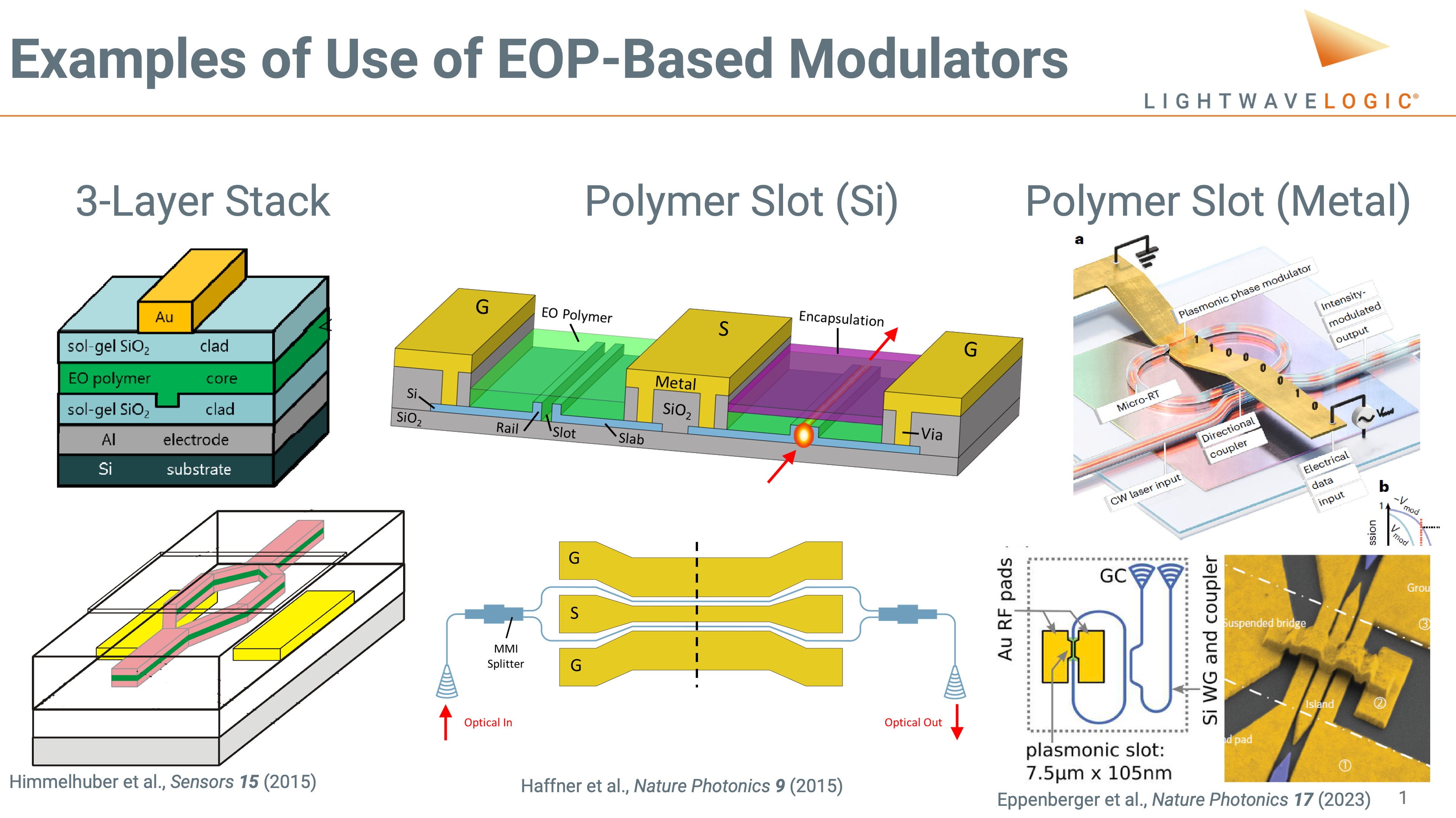
High performance EO polymers, boasting electro-optic coefficients exceeding 1000 pm/V and demonstrating ultra-fast modulation capabilities such as Vpi of <0.5V, compatibility with CMOS based fab PDKs, and devices as compact as 2 mm, offer compelling solutions for short-reach high-speed interconnects and low-power applications, though further improvements in long-term thermal stability are still needed.
BTO, known for high electro-optic coefficient, also shows potential for integration with silicon platforms; despite current challenges such as frequency dispersion and bias stability, it is poised to become a major candidate for next-generation ultra-high-speed optical interconnects.

SOH platform, which combines the mature fabrication processes of silicon photonics with the high-efficiency modulation properties of organic materials such as EO polymers, strikes a balance between speed and manufacturing compatibility, rapidly emerging as a leading technology direction for next-generation high-frequency optoelectronic integration.
We have also observed that a company in Taiwan is actively developing an SOH (Silicon-Organic Hybrid) platform, and has already introduced a 3.2T CPO (Co-Packaged Optics) solution based on this technology.
Moving forward, SemiVision will continue to provide deeper insights into SOH process technologies and share our findings with the industry.
The introduction of these new materials and associated platforms is poised to drive modulation rates beyond 200 Gbaud and toward 300 Gbaud, while simultaneously reducing drive voltages to below 1V, optimizing energy efficiency, and enabling further device miniaturization. This will open new possibilities for next-generation system architectures such as Co-Packaged Optics (CPO) and Near-Packaged Optics (NPO).

Against the backdrop of the rapid advancement of high-speed optical communication technologies, electro-optic (EO) polymer technology is increasingly emerging as a key enabler for upgrading data centers and artificial intelligence infrastructure. Particularly at the OFC50 conference, the industry engaged in in-depth discussions regarding the potential of EO polymers in 400G/lane and co-packaged optics (CPO) applications, as well as the future challenges that high-frequency modulators might face.
During this major technical event, Lightwave Logic, Inc., a technology company based in Englewood, Colorado, attracted widespread attention. The company is focused on developing and commercializing next-generation high-performance EO polymers, aiming to enhance transmission speeds and energy efficiency across data centers and telecommunications networks, with a special emphasis on meeting the high-speed data transfer demands of generative artificial intelligence applications.

Lightwave Logic’s core technology lies in its proprietary Perkinamine® electro-optic polymers, which offer high electro-optic coefficients, low power consumption, and ultra-fast response speeds, enabling data transmission rates exceeding 400 Gbps. In collaboration with Polariton Technologies, the company successfully demonstrated a plasmonic Mach-Zehnder modulator based on EO polymers, achieving 400 Gbps per channel transmission rates, with the potential to scale up to 800 Gbps, paving the way for future total bandwidths of 3.2 Tbps and 6.4 Tbps.
Overall, Lightwave Logic’s innovations and applications in the field of electro-optic polymers provide strong support for meeting future high-speed data transmission demands. In particular, the company demonstrates significant potential and promising prospects in high-bandwidth application scenarios such as generative artificial intelligence and data centers.

High Frequency Modulation: New Material — The Role and Technology Outlook of Lightwave Logic.
Against the backdrop of explosive global data traffic growth and the urgent emergence of Tbit/s-level data transmission demands, “High Frequency Modulation: New Material” has become a critical driver for the next wave of optical communication infrastructure upgrades.
At the OFC50 conference, the industry, for the first time at scale, engaged in extensive discussions on the potential of electro-optic polymers (EO polymers) for 400G/lane and co-packaged optics (CPO) applications, while also addressing the multifaceted challenges facing future high-frequency modulators—including power consumption, device size, thermal stability, and packaging compatibility.
A large number of technical papers published at the conference clearly reflected the industry’s growing expectations and investments in new material technologies as solutions to the bottlenecks of traditional silicon photonics platforms.
In the midst of this technological revolution, Lightwave Logic, Inc., has emerged as a major focal point. Lightwave Logic is dedicated to developing and commercializing next-generation high-performance electro-optic (EO) polymer materials, aiming to significantly enhance data transmission rates and energy efficiency for data centers and telecommunications networks, with a special focus on high-speed data exchange scenarios required by generative artificial intelligence (Generative AI).
Lightwave Logic’s core technology is its proprietary Perkinamine® electro-optic (EO) polymer platform. This material offers key advantages including a high electro-optic coefficient (r₃₃), low power consumption, and high-frequency response, making it suitable for manufacturing electro-optic modulators that can efficiently convert electrical signals into optical signals at extremely high speeds.
These capabilities enable data transmission rates exceeding 400 Gbps, with scalability toward 800 Gbps, 1.6 Tbps and 3.2Tbps platforms. Such platforms are aimed at supporting the next generation of large-scale generative AI data center clusters and campus network architectures, laying the foundation for future interconnect demands
Lightwave Logic adopts a business model based on technology licensing and co-development, entering into non-disclosure agreements (NDAs) with Tier-1 and Tier-2 strategic partners to jointly evaluate the application potential of its EO polymer technology across data center equipment, optical modules, and CPO (Co-Packaged Optics) platforms.
The company is committed to providing solutions that are simple and compatible with existing semiconductor wafer fabrication processes, with the goal of reducing the power consumption of thousands of optical components through advanced materials, while offering a sustainable evolutionary path for future bandwidth upgrades such as 3.2 Tbps and 6.4 Tbps, thus avoiding the high costs and risks traditionally associated with system upgrades.

In terms of enabling commercial deployment, Lightwave Logic has introduced a Process Design Kit (PDK) compatible with silicon photonic integrated circuits, successfully achieving seamless integration of its Perkinamine® materials with existing semiconductor manufacturing workflows.
The company has demonstrated the practicality and manufacturability of this PDK through collaborations with two semiconductor foundries, laying a strong foundation for commercializing EO polymer technology and enabling large-scale production.

Meanwhile, Lightwave Logic has also established collaborations with institutions such as ETH Zurich and Polariton Technologies to co-develop plasmonic Mach-Zehnder modulators (Plasmonic MZMs) based on EO polymers.
These modulators have already demonstrated single-channel transmission rates exceeding 1.6 Tbps. This achievement not only validates the technical feasibility of EO polymers for ultra-high-speed applications but also positions Lightwave Logic as one of the most closely watched emerging material suppliers in the fields of CPO and next-generation high-speed optical modules.
In summary, with global data center densities continuing to rise and generative AI computing scales exploding, the demands for bandwidth, energy efficiency, and device miniaturization in data interconnects are escalating dramatically.
Traditional silicon photonics technologies alone are increasingly unable to meet these future challenges. Through continuous innovation and rapid advancement in the EO polymer domain, Lightwave Logic is opening new possibilities for high-speed optical interconnects and CPO applications, providing a critical key for the optical communications industry to enter a new era characterized by higher frequencies, lower power consumption, and greater integration.
For Paid Members, SemiVision will discuss topics on
Leading a New Era of High-Frequency Optical Modulation with Electro-Optic Polymers
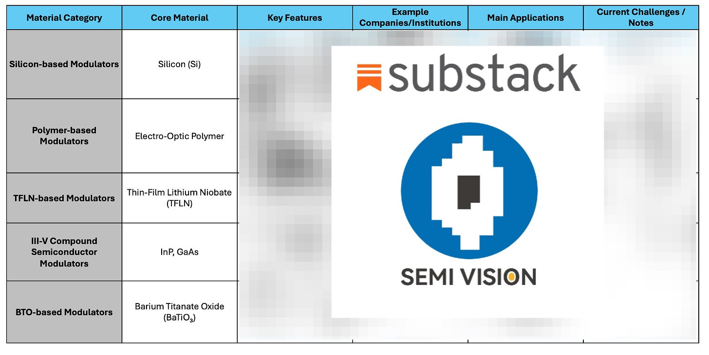
SemiVision Research: An Analysis of Modulator Material Classifications
Silicon-based Modulators
Polymer-based Modulators
Lithium Niobate-based Modulators
Core Characteristics and Technical Advantages for Lithium NiobateIII-V Compound Semiconductor Modulators
BTO-based Modulators
Key Features and Advantages for BTO-based Modulators
SemiVision Research: Overview of Next-Generation High-Speed Optical Modulator Materials and Technology Progress at OFC50