

The Material Code of High‑Speed SerDes Design: How CCL Choices Reshape PI/SI Integration and Bandwidth Limits
Original Articles By SemiVision Research (Marvell , Broadcom , MediaTek , TSMC , Nvidia , Delta , Foxconn )


800V HVDCTechnical Introduction
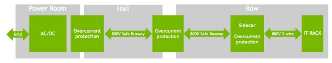
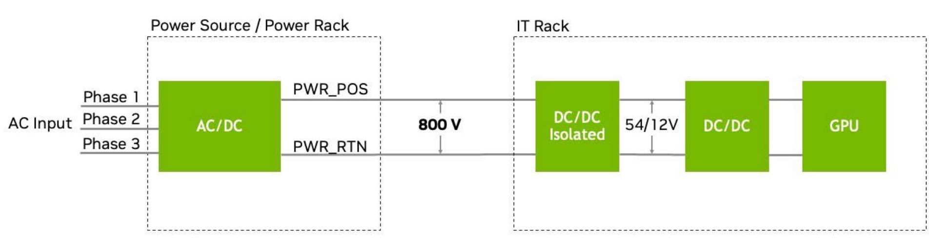
As AI workloads continue to grow exponentially, data center power requirements are rapidly escalating from hundreds of kilowatts to megawatt‑level per rack. Traditional 54 V in‑rack power distribution, designed for ~kW racks, reaches its physical and efficiency limits once per‑rack delivery nears ~200 kW, encountering issues such as bulky copper busbars, space constraints, and cumulative losses from multiple AC/DC and DC/DC conversions. NVIDIA’s emerging 800 V HVDC architecture addresses these challenges by converting 13.8 kV AC at the facility edge into 800 V DC, which is then delivered via high‑current busbars directly to compute racks. Within each rack, only a single DC/DC stage is required to step down to 54 V or 12 V for GPU core voltages. This streamlined design reduces in‑rack copper usage by up to 45 %, slashes conversion losses, frees up rack space, and lowers cooling overhead. When paired with optimized liquid cooling and centralized power conversion strategies, overall power delivery efficiency improves by approximately 5 %, marking a paradigm shift in enabling 1 MW‑class racks and beyond.
Supply Chain & Ecosystem
To accelerate this transition, NVIDIA has aligned with a cross‑section of industry partners across the AI power ecosystem. This includes power‑semiconductor leaders such as Analog Devices, Infineon, Navitas, ROHM, STMicroelectronics, Renesas, Texas Instruments, who are developing the GaN‑/SiC‑based switches and control ICs at the heart of the 800 V HVDC lodestar. Supporting these silicon efforts are module and system vendors like Delta, Flex Power, Lead Wealth, LiteOn, Megmeet, which design high‑voltage DC buses, rectifier units, and busbar assemblies. At the facilities layer, firms including Eaton, Schneider Electric, Vertiv are collaborating on DC‑centric power rooms, overcurrent protection schemes, and integrated UPS/PDU systems. Together, this ecosystem is addressing safety, fault isolation, thermal management, and repair standards required to make high‑voltage DC viable at scale. With the NVIDIA Kyber rack platform slated for production in 2027, this ecosystem is expected to deliver a full stack, MW‑scale AI data center power architecture.
NVIDIA 800 VDC Architecture Will Power the Next Generation of AI Factories
However, inside an AI chip, the operating voltage (VDD) of CMOS logic is only around 0.6–1.0 V, with threshold voltages (Vt) even below 0.8 V. Converting 800 V down to sub‑1 V in a safe, efficient, and low‑noise manner is a fundamental system challenge. This is where IVR (Integrated Voltage Regulator) technology becomes essential: IVRs move traditional board‑level VRMs into the package or even onto the die, delivering ultra‑stable power at very short distances, lowering PDN impedance, and enabling dynamic voltage scaling (DVS) to handle the large transient currents of AI workloads. This power chain—from HVDC to busbars, IVRs, and finally sub‑1 V CMOS—is the backbone of modern AI supercomputers. Without it, large‑scale AI clusters cannot operate reliably or efficiently.
Even once power delivery is stabilized, system design challenges continue. High‑density GPU motherboards must carry hundreds of high‑speed SerDes lanes and HBM memory interfaces, making the CCL (Copper‑Clad Laminate) materials of the PCB critical for signal integrity and system reliability. AI server boards often exceed 20–36 layers and must employ ultra‑low‑loss materials with low dielectric constants (Dk ≈ 3.2–3.5) and low dissipation factors (Df < 0.002), such as Megtron‑6 or Rogers 4350B, combined with heavy‑copper stack‑ups to sustain hundreds of amps of current and withstand tens of kilowatts of thermal load. Poor material selection or stack‑up design can lead to excessive insertion loss, eye‑diagram collapse, or board overheating, reducing long‑term reliability. Additionally, liquid‑cooling systems—whether direct‑to‑chip or full immersion—must be co‑designed with PCB stack‑ups, thermal interface materials, and rack‑level fluid loops to effectively dissipate heat. Only by integrating power delivery, PCB material design, thermal architecture, and high‑speed networking (such as NVLink or InfiniBand) can an AI data center achieve a truly scalable, high‑performance system. From wafer fabrication, advanced packaging (TSMC, Amkor, SPIL), testing, and module assembly to rack integration, building an AI supercomputer is a long and highly complex end‑to‑end process—every stage impacts overall efficiency and scalability, fully reflecting the precision and challenge of AI data center engineering.
In high-speed SerDes design, CCL (Copper-Clad Laminate) materials pose significant challenges to both Signal Integrity (SI) and Power Integrity (PI). Therefore, when evaluating and interpreting SerDes performance, it is essential to fully understand the material characteristics and their impact on channel loss.
In today’s high-speed digital system design, Signal Integrity (SI) and Power Integrity (PI) have become core factors influencing overall system performance and stability.
As SerDes (Serializer/Deserializer) channel rates evolve from 56G PAM4 to 112G, 224G, and even 400G PAM6, the effects of channel loss, crosstalk, reflections, and power noise on system Bit Error Rate (BER) and jitter are greatly amplified. Against this backdrop, CCL (Copper-Clad Laminate) materials play a critical role. They not only determine the insertion loss and overall performance of high-speed channels but also directly influence the impedance stability and thermal management of the PCB, serving as the critical bridge that links SI and PI considerations in next-generation SerDes design.

In our previous discussion, we explored in depth the critical role of Signal Integrity (SI) and Power Integrity (PI) in advanced AI chip design. These topics span not only the design of high-speed SerDes channels but also extend to the entire system-level Power Delivery Network (PDN) and signal transmission architecture.
For AI chips, where computational density, power consumption, and bandwidth requirements all surge simultaneously, any degradation in SI or PI directly leads to system performance bottlenecks, increased Bit Error Rate (BER), and even limits the scalability of the chip architecture.
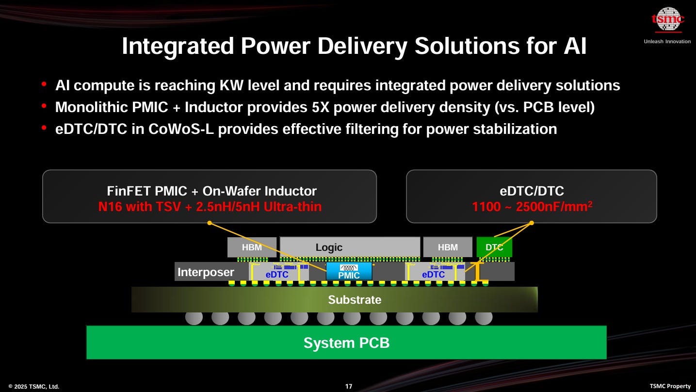
TSMC’s advanced CoWoS platform has already begun incorporating Integrated Voltage Regulator (IVR) technology, embedding voltage regulators directly into the package or chip. This approach, combined with high-performance Power Management ICs (PMICs) and precisely designed RF inductors, helps reduce power loop inductance, improve transient response, and suppress voltage ripple. At the same time, designers must account for effects such as the Q Factor to prevent resonances within the package from degrading high-speed power delivery. This level of fine-grained power integrity management is particularly critical for AI chips targeting large-scale training and inference workloads, where both SI and PI define the practical performance limits of next-generation data center systems.
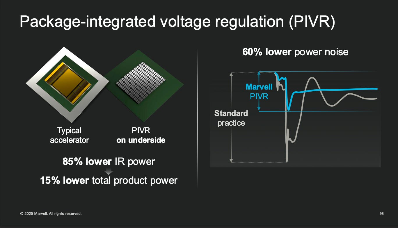
Marvell’s Package-Integrated Voltage Regulator (PIVR) technology, introduced in 2025, is a critical solution to the power delivery challenges faced by high-power AI and cloud data center chips. As AI processors surpass the multi-kilowatt power range, traditional board-level power delivery architectures encounter severe bottlenecks: long high-current, low-voltage paths, significant IR losses, slow transient response, and difficult-to-manage power noise. PIVR addresses these issues by integrating the voltage regulator directly into the chip package, minimizing power delivery distance, dramatically reducing parasitic inductance and voltage drop, improving IR losses by up to 85%, and lowering power loop noise by roughly 60%. This proximity-based power delivery method not only enhances transient response but also supports high-performance server platforms exceeding 4 kW, making it essential for high-speed SerDes, CXL, and optical-electrical co-packaged architectures.
Marvell’s PIVR (Package-Integrated Voltage Regulator) technology combines high-performance PMICs, ultra-thin ferrite inductors, and precise power filtering control, achieving current densities of 3–4 A/mm²—significantly higher than the 1.5–2 A/mm² typical of traditional solutions—while supporting real-time voltage regulation to reduce overall power consumption by roughly 15%. To accomplish this, Marvell has built a complete package-level power delivery ecosystem in collaboration with partners such as Ferric, Empower, and Infineon. Ferric’s ultra-compact thin-film magnetic IVR modules are only one-tenth the volume of conventional solutions, making them ideal for direct package embedding and drastically reducing parasitic effects. Empower’s FinFast architecture provides fast dynamic power control, further improving transient stability. Together, these innovations not only enhance power integrity (PI) by minimizing loop inductance and mitigating Q-factor resonance risks but also directly benefit signal integrity (SI), as cleaner and more stable power delivery reduces jitter and power-induced noise that can degrade SerDes eye openings and increase bit error rates (BER).
In practical applications, Marvell’s PIVR (Package-Integrated Voltage Regulator) technology is particularly critical for CoWoS, chiplet-based architectures, and Co-Packaged Optics (CPO) systems, where ultra-high-speed channels and low-noise power delivery are essential. Traditional board-level power architectures not only increase the burden of PCB decoupling capacitors, loop design, and thermal management but also limit the scalability of advanced AI chip architectures. By embedding IVRs directly into the package, PIVR frees valuable PCB space, simplifies power distribution network (PDN) design, and provides a superior power solution for next-generation high-density multi-chiplet systems. For AI training and inference servers, as well as cloud data center platforms that demand extreme performance and energy efficiency, Marvell’s PIVR technology represents not just an innovation in power delivery design but also a core strategy for maintaining the overall balance of signal integrity (SI) and power integrity (PI).
Extending this concept further, the same design philosophy applies to Silicon Photonics (SiPh) platforms and Optical Engine architectures. At the 2025 VLSI Symposium, TSMC introduced a comprehensive silicon photonics integration framework, where Photonic Integrated Circuits (PICs) and Electronic Integrated Circuits (EICs) are co-designed at the packaging level with holistic consideration of power delivery, thermal management, and signal interconnect performance. Since optoelectronic hybrid systems in 2.5D and 3D packages still rely on short- or medium-reach SerDes and high-speed channels to interface with the PCB, ensuring end-to-end channel consistency—from chip to package to board—has become a critical challenge for next-generation AI and data center system design.

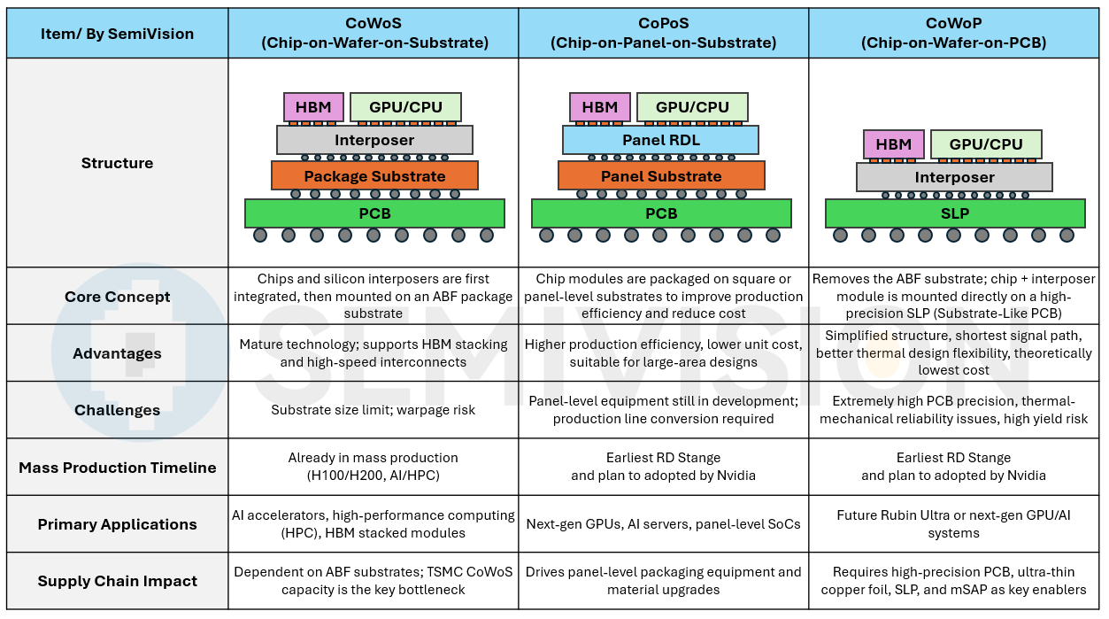
Ultimately, whether it involves logic chips, photonic engines, or stacked HBM memory, all signal and power paths must eventually traverse the PCB, making high-speed PCB design principles indispensable. This trend underpins the industry’s growing focus on advanced packaging-to-board integration strategies such as CoWoP (Chip-on-Wafer-on-PCB), combined with fine-line manufacturing processes like mSAP (Modified Semi-Additive Process), to shorten interconnect lengths and optimize overall system performance.
In the semiconductor world, a silent yet dramatic revolution is underway. As process nodes push into 3 nm and 2 nm, the true limits of chips are no longer defined solely by lithography resolution, but by the complex trade‑offs of economics, power, and system‑level design. The giants of the AI era—large language models, generative AI accelerators, and 1.6 Tbps high‑speed interconnects—are devouring the advantages of traditional monolithic SoC designs, forcing the industry to fully embrace chiplets, Co‑Packaged Optics (CPO), and 3D integration through hybrid bonding.
Tomorrow’s computing systems will no longer be single, monolithic engines. Instead, they will become intelligent infrastructures woven together by countless high‑speed chiplets, optical fibers, power delivery networks, and advanced cooling structures. At the heart of this transformation, CCL materials, PCBs, and advanced packaging (CoWoS, CoPoS, CoWoP) play a pivotal role. They not only determine signal transmission loss and integrity (SI) but also dictate power network stability and transient response (PI). Balancing multi‑layer high‑speed routing, complex PDNs, thermal management, and mechanical stress is now the core challenge for designers.
From Broadcom’s 224 G SerDes and Tomahawk 6, to Marvell’s PIVR power strategy, to MediaTek’s NVLink Fusion collaboration with NVIDIA—every step pushes the boundaries of extreme engineering and rewrites the philosophy of data center design. When CCL, PCB, CoWoS, CoPoS, CoWoP, SI, and PI all converge into a single design equation, the players who can find the perfect balance among power, bandwidth, materials, and ecosystem integration will ultimately define the winners of the AI era.
If you want to truly understand this deep transformation—spanning chips, packaging, and systems—and how top companies are shaping the semiconductor landscape for the next decade, this is content you simply cannot afford to miss.
For Paid Members ,SemiVision will discuss topics on
From 800 V to 0.8 V: Engineering the Next‑Generation AI Data Center
Powering the AI Era: From Grid‑Level HVDC to Sub‑Volt Silicon
Breaking the Bandwidth Barrier: How CCL and IVR Redefine SI/PI for 224G SerDes and PCIe 7.0
Challenges of PI/SI in High-Speed Transmission: The Evolution of PCB in the SerDes Era
Market Implications in Nvidia’s AI GPU
PI/SI Design Challenges under Rising SerDes Bandwidth
Signal Integrity (SI) Challenges
Power Integrity (PI) Challenges
System-Level Challenges of SerDes Bandwidth Scaling
Summary and Industry Implications
Upstream Material Segment – CCL and Electronic Glass Fabric
PCB Manufacturing – Advanced Processes and System Co-Design
A Value Chain Reshaped by AI Compute Demand
Resonance and Impedance Traps in Power Integrity: Rethinking “Lower Impedance Is Always Better”
The Physical Nature of Resonance
Quality Factor (Q-Factor) and Impedance Peaks
CCL Materials and Signal/Power Integrity Challenges in High-Speed SerDes Design
PCB CCL Materials and Channel Loss
PAM4 and PCIe Gen6 Channel Loss
Enterprise Strategies in High‑Speed Connectivity: Broadcom, Marvell, and MediaTek
Industry Update: Marvell
Industry Update: Broadcom
Industry Update: MediaTek
Impact of Integrated Voltage Regulators (IVR) on SI/PI
