

The Packaging Evolution Trilogy: Hybrid Bonding, Fluxless TCB, and 3D Stacking Ignite a Supply Chain Reshuffle
Original Articles By SemiVision Research ( IEEE ECTC , IEEE IITC ,BESI , TSMC , UMC ,Nvidia, AMD , Intel ,TEL , Suss ,EVGroup , K&S , ASMPT ,AMAT , SHIBAURA ,SET , NYCU ,ITRI)


The semiconductor industry is currently standing at a critical inflection point of transformation and restructuring. As AI computing demand grows exponentially, traditional Moore’s Law scaling can no longer singlehandedly sustain breakthroughs in system-level performance. In this context, advanced packaging technologies are rapidly evolving from a “backend process” into the core enabler of system integration and architectural innovation.
In this compute-centric technological race, whether it’s high-end AI accelerators in data centers or compact Edge AI chips deployed at the network edge, all rely on packaging solutions with higher precision, greater integration, and wider bandwidth. From TSMC’s CoWoS/SoIC platforms to the emerging heterogeneous integration strategies pursued by UMC, ASE, and SPIL, and from equipment leaders like BESI, EVG, and AMAT advancing Hybrid Bonding, to China’s aggressive investments in domestic supply chains—the direction is clear: the future lies in 3D stacking + chiplet architectures + heterogeneous integration + silicon photonics.

This report series will explore the future trajectory and challenges of advanced packaging across four key dimensions: market scale, technical bottlenecks, supply chain evolution, and equipment ecosystem dynamics. We will specifically focus on the following strategic themes:
Diverse packaging demands for Edge AI: Which packaging architectures are best suited for low-power, space-constrained edge applications?
The potential of Wafer-on-Wafer (WoW) integration: Can it outperform other solutions in high-density, low-power scenarios?
Material and packaging challenges in silicon photonics: How should the industry prepare for photonic-electronic convergence?
Global competition in Hybrid Bonding supply chains: Who is driving the process transformation, and who is closing the gap?
Breakthroughs and integration among Chinese players: From homegrown equipment to production line deployment—will we see regional reshaping of the packaging supply chain?
As AI becomes a foundational infrastructure, as computation extends beyond the cloud, and as heterogeneous integration and photonic convergence become the new normal, packaging technology is no longer just an engineering challenge—it’s a strategic battleground. In the future, the question won’t just be “Who can build the chip?”, but rather “Who can integrate everything together most effectively?”
And that revolution is already underway.
Driving the Next Era of Advanced Packaging: AI, Silicon Photonics, and Co-Packaged Optics
As AI workloads rapidly scale beyond trillions of parameters, the role of advanced packaging has evolved from a passive interconnect layer into a performance-critical design platform. Today’s AI chips are no longer monolithic systems but rather chiplet-based architectures requiring ultra-high bandwidth, low-latency, and thermally efficient integration.
This has led to the convergence of several advanced technologies:
AI-driven Packaging Requirements
Modern AI chips—especially those supporting generative inference and large-scale training—demand:
2TB/s chip-to-memory bandwidth
<1ns interconnect latency
700W cooling capacity per package
To meet these demands, chipmakers are adopting 2.5D and 3D packaging with HBM stacks, ultra-fine pitch hybrid bonding, and advanced thermal materials.

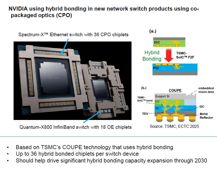
Silicon Photonics and Co-Packaged Optics (CPO)

As electrical I/O (SerDes) begins to plateau at ~200G/lane, optical I/O becomes essential:
Silicon Photonics enables monolithic integration of optical engines with CMOS logic, reducing energy per bit and improving signal integrity over long distances.
Co-Packaged Optics (CPO) moves the optical engine into the package, eliminating the power-hungry retimers and signal loss from board-level interconnects. Vendors like NVIDIA, Marvell, Ranovus, and Broadcom are deploying CPO in next-generation switches and AI systems.
However, CPO introduces new packaging challenges: sub-micron optical alignment, material stack thermal expansion mismatch, and co-integration of photonic dies with high-power logic.
Packaging as a System Platform
Major foundries and IDMs are now positioning packaging as a system-level platform:
TSMC offers SoIC-X, CoWoS-R, and InFO-L for chiplet-based and memory-centric AI packaging.
Intel is investing in EMIB, Foveros Direct, and glass substrates for ultra-large die integration and improved signal/power delivery.
These platforms are designed to accommodate hybrid bonding, optical interconnects, and integrated power delivery networks, effectively turning the package into a critical layer of the compute hierarchy.
As hybrid bonding matures and packaging architectures absorb optical and power delivery functions, the entire value chain—from foundries to OSATs to equipment vendors like BESI, EVG, AMAT, ASMPT—is being reshaped around the demands of AI infrastructure.
As advanced packaging technologies continue to evolve, Fluxless Thermo-Compression Bonding (TCB) is rapidly emerging as a critical process for supporting AI chips, high-bandwidth memory (such as HBM), and silicon photonics modules. Traditional TCB relies on flux and reflow processes to facilitate solder wetting and oxide removal. However, in fine-pitch bonding—particularly below 40μm—this approach often leads to voids, residual contamination, and reduced reliability, falling short of the precision requirements.
Fluxless TCB, on the other hand, replaces flux with plasma activation, reducing atmosphere heating, and surface cleaning, while utilizing highly controlled temperature and pressure to achieve Cu-to-Cu or Sn-based bonding. This technique significantly reduces residual contamination, improves bond cleanliness and yield, and enhances signal integrity and thermal performance—making it particularly well-suited for high-integration, high-bandwidth, and high-power packaging structures.
In packaging schemes like CoWoS-L, which target large chiplets and high-end logic dies, Fluxless TCB not only provides a more stable bonding interface but also aligns with industry trends toward contamination-free, high-reliability, and increased packaging density. Due to the process’s stringent requirements for bump height uniformity and surface flatness, Z-height control and bonding compensation technologies are essential. Equipment lacking micron-level height control capabilities will struggle to handle fine bump alignment errors, ultimately compromising yield and long-term reliability.
In contrast, Hybrid Bonding employs solder-free techniques that simultaneously bond metal and dielectric layers, enabling superior electrical performance at higher bandwidths and smaller pitches. Fundamentally different from fluxless TCB, Hybrid Bonding is more suitable for next-generation 3D integration requirements.
Overall, Fluxless TCB and Hybrid Bonding represent the two primary technological pillars driving future heterogeneous integration, high-bandwidth, and high-density packaging. The ability to precisely control bonding quality and enhance process flexibility will determine their central roles in next-generation advanced packaging architectures.
In the rapidly evolving field of advanced packaging, Taiwan’s semiconductor supply chain is undergoing a strategic shift, driven by explosive demand from AI and high-performance computing (HPC) applications. While TSMC remains the dominant provider of advanced packaging capacity—particularly for AI chips relying on CoWoS—other Taiwanese players such as UMC and ASE (including SPIL) are emerging as critical alternative sources, especially for edge AI and customized applications that require diverse packaging approaches.
UMC Secures Qualcomm’s Advanced Packaging Order Amid TSMC Supply Constraints
UMC’s recent win of Qualcomm’s advanced packaging order marks a major turning point for Taiwan’s role in the global AI and HPC packaging landscape. The significance of this development lies not merely in a single technical breakthrough, but in the broader backdrop of capacity constraints—specifically, the severe bottleneck in TSMC’s CoWoS production lines.
Due to overwhelming demand from leading AI players like NVIDIA and AMD, TSMC’s advanced packaging capacity is fully booked through 2024–2025. As of mid-2024, CoWoS monthly output has expanded from 13,000 wafers (end of 2023) to around 30,000–35,000 wafers. TSMC plans to grow this to 70,000–80,000 wafers per month by the end of 2025, and eventually reach 100,000–120,000 wafers per month by 2026. However, the pace of expansion still falls short of hyperscaler demand, forcing medium-sized customers like Qualcomm to explore alternative foundry partners.
It is in this context that UMC has seized a rare opportunity to rise in the advanced packaging segment. In fact, UMC has long been quietly investing in key technologies such as through-silicon vias (TSVs), precision interposer manufacturing, and wafer-on-wafer (WoW) hybrid bonding. The collaboration with Qualcomm is expected to begin pilot production in the second half of 2025 and move to volume production in 2026. Notably, in this project, UMC will handle packaging, while wafer fabrication remains with TSMC—highlighting an emerging trend of competitive yet cooperative specialization.
UMC’s Ecosystem Advantage: Vertical Integration and Platform Synergy
UMC’s success is not solely the result of external capacity shifts. It also reflects its ability to offer a vertically integrated packaging platform, built through partnerships with companies like Faraday , Silicon Integrated Systems (矽統), Winbond, and ASE. This ecosystem spans from wafer processing and chip design to memory integration and test, enabling customers to accelerate heterogeneous integration and address challenges in high-bandwidth and high-power packaging architectures.
Faraday plays a key role as an advanced packaging design service provider, focusing on processes at 16nm and above. It offers customized interposer fabrication with TSV support. SiS (Silicon Integrated Systems) specializes in high-speed interface chips and is poised to integrate with 2.5D/3D packaging technologies to penetrate AI and HPC supply chains. Winbond focuses on high-bandwidth memory (such as CUBE) and hybrid bonding, with small-volume shipments starting in 2024 and meaningful revenue expected in 2025.
AI Infrastructure Reshapes Global Packaging Supply Chains
The UMC–Qualcomm collaboration symbolizes a broader trend: IC design houses are reconfiguring their supply chain strategies. As sovereign AI infrastructure builds out globally, the battle for advanced packaging capacity is intensifying. While TSMC retains a technical edge in platforms like CoWoS and SoIC, its bottlenecks and customer concentration are creating space for competitors like UMC, ASE, and Samsung to gain ground.
This is not a case of replacement, but of diversification and supply chain flexibility. Qualcomm’s engagement with UMC does not imply a departure from TSMC—it’s a strategic move to secure a secondary, reliable packaging source as long as TSMC remains oversubscribed. Looking forward, as 3D packaging and chiplet architectures become mainstream, providers with full-stack integration, robust partnerships, and high-volume experience will command increasing influence. UMC is now one of the most important players to watch in this new chapter of advanced semiconductor packaging.
For Paid Members , SemiVision will discuss topics on
Fluxless TCB vs. Hybrid Bonding: Industry Update
CoWoS-L and the Critical Role of Fluxless TCB in Advanced Packaging
Fluxless TCB and Hybrid Bonding in Advanced Packaging: Strategic Insights from TSMC, K&S, BESI, and ASMPT
Z-Height Control and the Equipment Race for Fine-Pitch Packaging
AI as the Primary Growth Engine for the Semiconductor Industry: BESI’s Outlook and Market Strategy
Seven Key Application Segments Driving AI Semiconductor Demand
BESI’s Positioning: Targeting the Core of AI-Driven Growth
BESI Focuses on Four Key End Markets: AI-Driven Architecture Driving Broad-Based Equipment Demand
A New Paradigm Beyond Moore’s Law: BESI Drives Chiplet and 3DIC Packaging Revolution with Hybrid Bonding and TCB
A New Paradigm for Data Center Chips: Chiplet Architecture and Hybrid Bonding Go Mainstream
Packaging as the Core Weapon for Chip Differentiation
AMD Leads the Chiplet Revolution: From Data Centers to Gaming Desktops
Accelerating Die Attach Innovation for Multi-Chip Systems: From Monolithic Integration to 3D Chiplet Packaging
Diverse Integration Demands of AI Chiplet Packaging: Besi’s Perspective on Advanced Packaging Evolution
Accelerating the Era of AI Packaging: A Comprehensive View of BESI’s Advanced Packaging and Chiplet Architecture Solutions
Hybrid Bonding: The Preferred Technology for High-Performance Chiplet Stacking
Intel Leverages Hybrid Bonding to Drive Next-Gen Datacenter Processors
Hybrid Bonding Enters Pre-Mass Production Phase with Broadcom and Apple Leading the Way
Hybrid Bonding Unlocks Value in Emerging CPO Applications
Reshaping the AI Chip Packaging Era: From Hybrid Bonding to the Full Evolution of the Chiplet Architecture
CPO and Photonic Integration Drive a Packaging Revolution
Hybrid Bonding: Unlocking the Future of HBM and Logic Integration
Smartphones Embrace Chiplet Packaging: A Dual Revolution in AI and Advanced Packaging
Overview and Trends of Hybrid Bonding Technology
Wafer-to-Wafer (W2W) vs. Die-to-Wafer (D2W) Hybrid Bonding
Latest Developments among Key Hybrid Bonding Equipment Suppliers
BESI (BE Semiconductor Industries):Global Leader in Precision D2W Hybrid Bonding and High-Yield Production Platforms
EV Group (EVG):Market Leader in Comprehensive Wafer Bonding and W2W Hybrid Bonding Solutions
Applied Materials (AMAT):Process Giant for Hybrid Bonding with Front-End Integration and Materials Mastery
Tokyo Electron (TEL):End-to-End Solution Provider for Wafer Cleaning, Bonding, and Thin Wafer Processing
ASM Pacific Technology (ASMPT):Automation Pioneer in Cu-to-Cu Bonding and Scalable 3D Packaging Equipment
SET (Smart Equipment Technology):Niche Expert in Ultra-High Precision D2W Hybrid Bonding Systems
Shibaura Mechatronics:Early Commercializer of Hybrid and Fusion Bonding with Dual-Head High-Throughput Platforms
SUSS MicroTec:Innovator of Modular Bonding Solutions Supporting Both W2W and D2W Integration
