

TSMC's N2 and the Power of PPACt: Driving the Future of Semiconductor Innovation
How TSMC's N2 Process Node Leverages PPACt to Lead in Performance, Efficiency, and Market Competitiveness

N2 Process at 2nm Begins Mass Production This Year
The image below shows TSMC's process node evolution over time. The red dots highlight the nodes TSMC introduced ahead of its competitors.
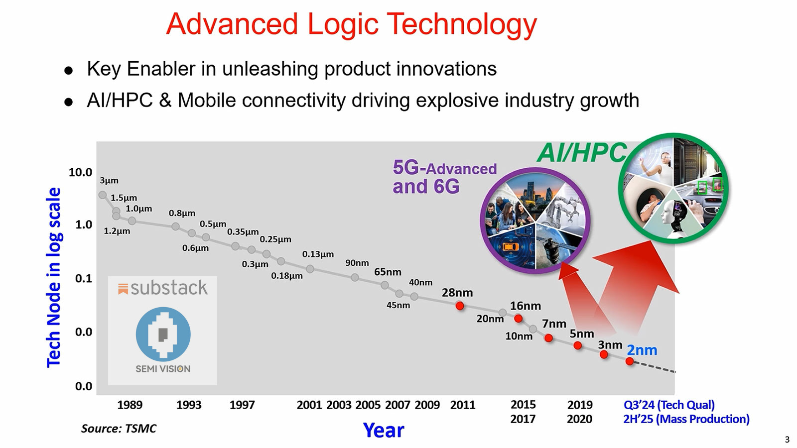
Since 16nm, TSMC has almost entirely dominated the field. However, before the 28nm generation, TSMC lagged behind competitors like UMC, with certain periods of notable delays. It has only been in the last decade or so that TSMC has achieved its unparalleled position in the semiconductor industry.
For instance, in the case of the 20nm node, Intel's 22nm was introduced earlier. Even for the 10nm node, while Intel struggled with high-volume production, the start of mass production was technically earlier than TSMC's. Similarly, TSMC's lead with the 28nm node was largely due to Intel skipping this node altogether (jumping from 32nm to 22nm).

When compared to the 28nm generation, the 2nm generation demonstrates remarkable improvements:
15x better performance-to-power ratio.
140x better performance-to-power ratio per unit area.
These impressive numbers are partly due to the significant technological advancements since the 28nm generation.

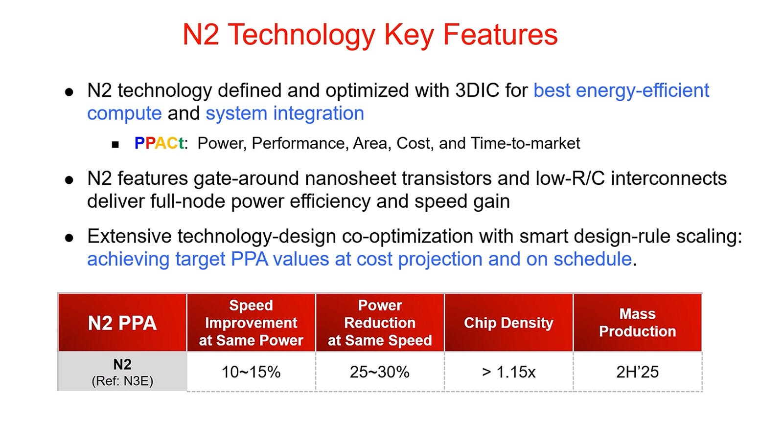
The first iteration of the 2nm node, N2, will soon be followed by products beyond Apple's lineup. Compared to N3E, which is about to enter mass production, N2 offers the following performance improvements:
10–15% faster at the same power consumption.
25–30% lower power consumption at the same clock frequency.
15% higher transistor density.
The performance metrics of the N2 g
The performance metrics of the N2 generation come from various sources. Initially, they were based on estimates, simulations, and design targets. However, the current data is more reliable as it comes from the Technical Qualification stage, meaning the figures have been validated to a higher degree of accuracy.

From PPA to PPACt Optimization
A distinctive feature of the N2 generation is its optimization framework evolving from PPA (Power, Performance, Area) to PPACt.
What is PPACt?
PPACt (Performance, Power, Area, Cost, and Time to Market) is crucial because it defines the key factors that drive semiconductor advancements and the competitiveness of chip manufacturers. Here’s why each component of PPACt matters:
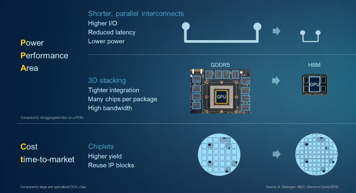
1. Performance (P) – Faster and More Efficient Computing
Why it matters: As applications in AI, HPC, and gaming demand more computing power, improving chip performance ensures better processing speed and efficiency.
Example: AI models like ChatGPT require high-performance GPUs and accelerators to process vast amounts of data quickly.

Source: TSMC
2. Power (P) – Energy Efficiency and Sustainability
Why it matters: Lower power consumption extends battery life in mobile devices and reduces energy costs in data centers.
Example: Companies like Apple prioritize power efficiency in their M-series chips for longer battery life in MacBooks.


3. Area (A) – Higher Transistor Density and Compact Designs
Why it matters: Smaller chips with more transistors per unit area enable more powerful devices without increasing size.
Example: Advanced nodes like 3nm allow smartphone chips to pack more transistors in a smaller footprint, boosting performance.
4. Cost (C) – Affordable Manufacturing and Market Competitiveness
Why it matters: Lower production costs enable companies to price products competitively while maintaining profit margins.
Example: TSMC and Samsung continuously optimize their manufacturing processes to reduce wafer costs.
5. Time to Market (t) – Speed and Agility in Innovation
Why it matters: In the fast-evolving tech industry, companies must rapidly bring new chips to market to stay ahead of competitors.
Example: NVIDIA and AMD race to launch new GPUs ahead of each other to dominate the gaming and AI acceleration markets.

Source: TSMC
PPA Optimization:
Traditionally, PPA has been the key to process optimization, focusing on the balance between power efficiency, performance, and chip area. Typically, trade-offs must be made:To prioritize performance, higher voltage and larger, high-speed transistors are used.
For power and area efficiency, lower voltage and high-density transistors are preferred. The balance depends on the desired performance relative to power consumption and chip size.
PPACt Optimization:
Recently, cost (optimization effort required) has been added to this framework, forming PPAC. With N2, Time-to-Market has now become a critical factor, transforming it into PPACt. This includes how efficiently the design-to-production timeline can be streamlined.
The phrase "Extensive technology-design co-optimization with smart design-rule scaling" reflects this new focus. It emphasizes smarter design-rule scaling and co-optimization between technology and design, allowing for shorter development cycles.
Example: Broadcom's TSMC N7 Challenges
A historical example highlights the importance of reducing time-to-market. When Broadcom designed the processor (an Arm v8-based custom core) on TSMC's N7 node, they faced significant challenges. The process involved four iterations of physical design and simulations, taking almost a year to complete. Each cycle of physical design, simulation, bottleneck identification, optimization, and resimulation took around three months.
This lengthy optimization process is no longer viable in today's competitive semiconductor landscape. The introduction of PPACt optimization in the N2 process aims to eliminate such inefficiencies, enabling faster and smarter design-to-production transitions.