

TSMC N3 and N2 Nodes: Shaping the Next Era of Chip Manufacturing
Advancing from 3nm to 2nm with GAA FinFET Technology and Integrated Packaging Solutions

TSMC mentioned in its Q3 2024 earnings call that customer demand for the 2nm process has exceeded expectations. In this analysis, we explore why the 2nm logic process is gaining such popularity. The primary reasons are as follows: First, the transition from the FinFET structure to the new Nanosheet GAA FinFET structure brings significant improvements in PPA (Power, Performance, and Area). PPA is a crucial metric for evaluating process performance in terms of power consumption, performance, and chip area. Additionally, the N2 process integrates Chiplet design, which substantially reduces transistor power consumption, making it highly attractive to many companies.
The N2 process is not only TSMC's flagship process for the future but also marks its first adoption of GAA FinFET technology. The upcoming 1.6nm process will continue to utilize the GAA FinFET architecture. Furthermore, we recognize the critical integration of advanced packaging technology with logic processes. Under this new process architecture, special attention must be given to the impact of AI chips on the development of the 2nm logic process, as well as key transitions when moving from the 3nm to the 2nm logic process, including changes in EUV layer count, materials, structures, pricing, and customer migration.
Introduction to TSMC's 3nm Process
After understanding the key definitions of logic processes, we now introduce TSMC's 3nm logic process technology.
Why Choose the 3nm Logic Process?
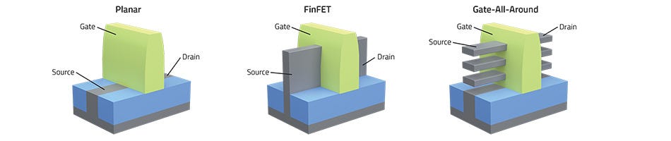
The primary reason for choosing the 3nm logic process is that TSMC continues to utilize the FinFET structure for this node, whereas the transition to the 2nm process marks the adoption of the GAA FinFET structure. Therefore, moving from the 3nm to the 2nm logic process represents a significant transformation in 3D FinFET architecture—shifting from the traditional 3D FinFET to the 3D GAA FinFET structure.
Introduction to TSMC's 3nm FinFET Platform
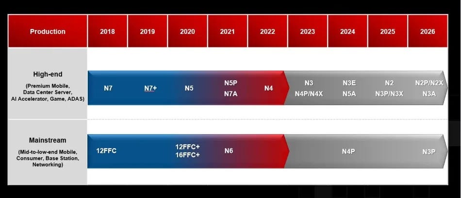
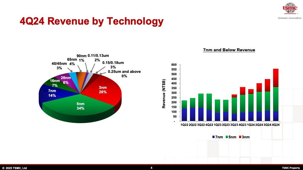
To begin, we provide a brief introduction to TSMC’s 3nm FinFET platform. In 2022, TSMC became the industry leader by successfully achieving high-volume production of its 3nm FinFET (N3) process technology. N3 represents the most advanced semiconductor logic process technology in the industry, offering superior performance, power efficiency, and area (PPA). It is a full-generation advancement following the 5nm (N5) process technology.

Following the introduction of the N3 process, TSMC further enhanced its technology portfolio by launching the N3E and N3P process nodes, which offer improved power efficiency, performance, and transistor density. Additionally, TSMC provides a broad range of process solutions to meet diverse customer demands, including the N3X process, designed specifically for high-performance computing (HPC) applications, and the N3AE solution, tailored for automotive customers to enable early adoption of the industry’s most advanced process technologies.

Within the N3 process family, the variations—N3E, N3P, and N3X—are developed to accommodate different device characteristics. For instance, the process requirements for HPC applications differ from those used for smartphone application processors (AP), leading to the optimization of each variant for specific applications.
TSMC N3 Family

The differences in the N3 process have a significant impact on the number of mask layers used and the overall cost.
Performance Comparison of the N3 Process

We can now provide a brief overview of the customers utilizing TSMC's N3 process.
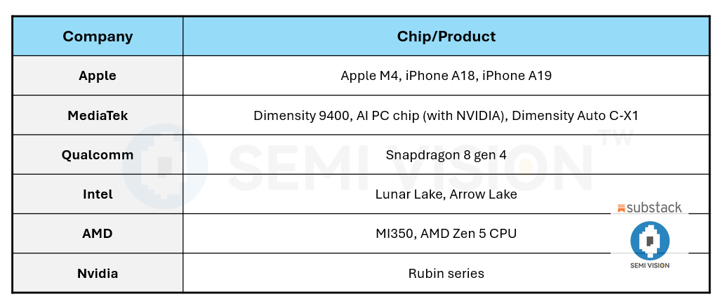
TSMC's N3 process has been adopted by several leading technology companies across various applications. Apple utilizes the N3 process for its M4 chips and iPhone processors, including the A18 and A19. MediaTek leverages N3 for its Dimensity 9400 chips, AI PC chips in collaboration with NVIDIA, and Dimensity Auto C-X1 chips for automotive applications. Qualcomm applies the N3 process for its Snapdragon 8 Gen 4 processors, while Intel uses it for their Lunar Lake and Arrow Lake platforms. AMD employs the N3 process for their MI350 and Zen 5 CPU products, and NVIDIA integrates it into their Rubin series. This widespread adoption highlights the versatility and advanced capabilities of TSMC's N3 technology.

The N2 process is not only TSMC's future flagship process but also marks TSMC's first adoption of the GAA FinFET architecture. The upcoming 1.6nm process will also follow the GAA FinFET design. Furthermore, we understand that advanced packaging must be integrated with logic processes. Under this new architecture, we need to carefully monitor the impact of AI chips on the development of the 2nm logic process. Additionally, we must conduct an in-depth analysis of the transitions from the 3nm to the 2nm process, including changes in EUV layer counts, materials, structures, costs, and customer migrations.
Moreover, TSMC, Intel, and Samsung are actively investing in GAA FinFET technology, highlighting the competitive dynamics in this field.

Introduction to TSMC's 2nm Process
Having briefly reviewed the evolution of TSMC's 3nm logic process, we now provide an overview of TSMC's 2nm logic process. Starting with the 2nm node, TSMC adopts Nanosheet technology, also referred to as GAA technology, specifically the Nanosheet GAA FinFET structure. This technology extends from the existing FinFET architecture.

The GAA FinFET technology has been a focus for Intel, Samsung, TSMC, and IBM, all of which published papers in 2022 discussing the transition from FinFET to GAA FinFET as a crucial step in the evolution of logic processes. Similar to the shift from planar MOSFETs to FinFETs, the move to Nanosheet GAA transistors requires overcoming numerous challenges in process integration. Fortunately, Nanosheets are considered a natural evolution of FinFETs, allowing many process modules developed and optimized for FinFETs to be reused. GAA transistors are essentially FinFET transistors rotated 90 degrees, with horizontal rather than vertical channels. These GAA channels are formed using multiple epitaxial layers and selective material removal techniques.
Below, we highlight the four key process steps that show the most significant differences between these two architectures, each requiring specific innovations. We will explore these aspects in greater detail in the future.
TSMC's 2nm (N2) technology development is progressing according to plan and achieving excellent results. N2 technology employs the first-generation Nanosheet transistor architecture, delivering performance and power efficiency improvements across the full process node. High-volume production is expected to begin in 2025.

Key customers have already completed the design of 2nm silicon intellectual property (IP) and are now conducting validation. Additionally, TSMC is developing low-resistance buried power rails and ultra-high-performance metal-insulator-metal (MIM) capacitors to further enhance the performance of its 2nm process technology.
TSMC's N2 Technology Overview
When TSMC’s N2 technology enters high-volume production in 2025, it will become the most advanced semiconductor technology in the industry in terms of density and energy efficiency. Featuring a cutting-edge nanosheet transistor structure, N2 delivers generational improvements in both performance and power efficiency to meet the growing demand for energy-efficient computing. N2 and its derivative technologies will further expand TSMC's technological leadership through sustained strategic enhancements.
N2 Capacity Outlook and Demand
TSMC has high expectations for N2 production capacity. During its Q3 2024 earnings call, TSMC noted that the increasing demand driven by HPC and AI applications is resulting in more use cases for the 2nm process.
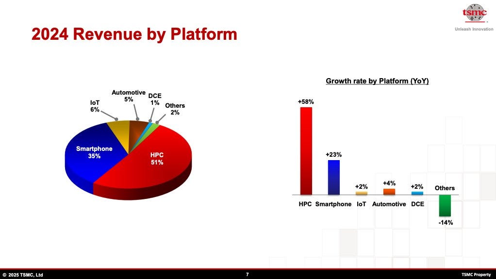
However, the adoption of chiplet designs may reduce demand for 2nm nodes. In response to this concern, TSMC CEO C.C. Wei clarified that chiplets will not decrease the demand for 2nm technology. In fact, HPC customers' demand for N2 exceeds that of N3. To address market needs, TSMC is preparing additional capacity for A16/N2 processes.
Chiplet designs at the 2nm level require close collaboration with EDA suppliers. TSMC's OIP (Open Innovation Platform) forum has highlighted strong partnerships with companies like Cadence and Synopsys, emphasizing their critical role in supporting advanced logic processes and packaging technologies.
Challenges in Advanced Packaging and Chiplet Design
We plan to further explore the role of EDA suppliers, as modern logic processes must be integrated with advanced packaging. The evolution from InFO and CoWoS to future technologies like 3D stacking (SoIC) and chiplet design presents significant challenges for EDA suppliers. One key challenge is the introduction of backside power delivery in the A16 process. This innovative technique requires separating signal lines and power lines during fabrication, adding substantial complexity. Integrating advanced packaging and chiplet designs will only further increase the overall manufacturing difficulty.
Future AI Chip Design
We are also conducting in-depth research on AI chip design, focusing on AMD’s MI-series products and NVIDIA’s chip architectures. This topic is extensive, as future AI chip designs must account for factors such as chip size, packaging, thermal management, and the use of HBM. These considerations are closely tied to technologies like SerDes, chiplet IP, and heterogeneous integration.
In future discussions, we will provide detailed insights into these areas to better understand the interplay between advanced processes, packaging, and AI chip development.